Appendix II: Link
and the use of a single positive
supply. Also included is a list of
the various options and their
definitions.
mode (M20SEL) and speed
selections (DIV0,DIV1) are
grouped together under the label
‘options.’ A power-on reset is
available to the user to reset the
link during startup.
Configuration Examples
This section shows some
application examples using the
HDMP-1022/1024 chipset. Refer
to I/O Definition for detailed
circuit-level interconnection.
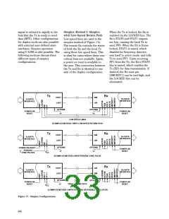
Duplex/Simplex
Configurations
The following describes the
common setups for the link. In all
cases, the DIN and LIN are
differential high speed lines, and
unused leads should be terminated
with 50 Ω AC coupled to ground.
Since the data stream has no DC
component, a coupling cap of
0.1 µF is recommended for the
DIN and LIN inputs.
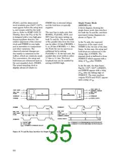
When the Tx has acquired lock to
the incoming STRBIN at the
This guide is intended to aid the
user in designing G-LINK into a
system. It provides the necessary
details of getting the system up,
without the detailed description of
the inner circuitry of the chip set.
frame rate, the LOCKED pin is
activated, which enables the Rx.
At this state, both STAT0 and
STAT1 are low, forcing the Tx to
send FF0, which is a square wave
pattern used by the remote Rx to
acquire frame lock. When the
local Rx has acquire frame lock,
STAT1 is set high to first turn off
its own frequency detector
(FDIS), then sets itself to active
mode (ACTIVE), and tells the
local Tx to send FF1 to signal the
remote Rx that the local pair is
ready. Likewise, when the remote
pair is ready, the local Rx will
receive FF1, causing STAT0 to go
high, which asserts the enable
data (ED) pin on the Tx. The ED
The first section is a description
of the various configurations for
duplex and simplex operation.
The second section describes the
interface to both single frame and
double frame mode. Following
that is a section on the integrating
capacitor and power supply
bypassing recommendations.
Next is a guide to the various
types of electrical I/O connec-
tions. The final section is a
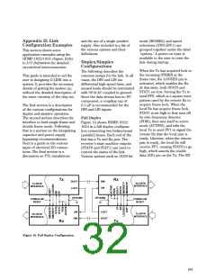
Full Duplex
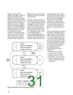
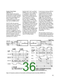
Figure 16 shows HDMP-1022/
1024 in a full duplex configura-
tion connecting two bidirectional
(parallel) buses. Each end of the
link has a Tx and Rx pair. The
receiver’s state machine outputs
(STAT0 and STAT1) are used to
control the status of the link.
Various options such as 16/20 bit
discussion on TTL translations
Tx
Rx
DOUT
LOUT
DIN
Rx DATA
INTERFACE
Tx DATA
INTERFACE
LIN
OPTIONS
OPTIONS
POWER-ON
RESET
POWER-ON
RESET
LIN
DIN
LOUT
DOUT
Tx DATA
INTERFACE
Rx DATA
INTERFACE
Rx
Tx
Figure 16. Full Duplex Configuration.
647

 AGILENT [ AGILENT TECHNOLOGIES, LTD. ]