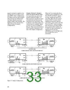
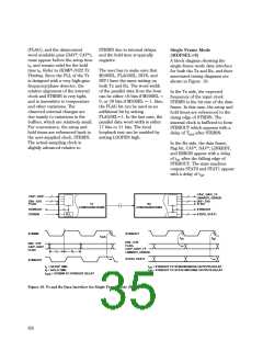
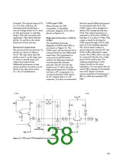
Simplex Method II. Simplex
with Periodic Sync Pulse.
Another configuration of simplex
operation is shown in Figure 17b.
For frame lock, the Rx normally
relies on either FF0 or FF1. In
this example, the fill frame FF of
the Tx is forced high with a
connection to ground, and the
enable data pin ED is pulsed
periodically to force the Tx to
send FF1. During this pulse,
however, the link is not available
for data transmission.
The high-speed serial line is
brought into the receiver through
the LIN input, and a reference
clock at the frame rate is
between the two frequencies in
order to guarantee a lock within a
reasonable time. In theory, a
perfect match could result in no
lock due by causing the receiver
to consistantly try and lock at the
same non-master transition point
in the incoming frames. For-
tunately there is no such thing as
a perfect match in the real world.
It is recommended to select
connected to the DIN input.
The Rx uses the reference clock
for frequency acquisition. Upon
frequency lock, STAT1 goes high,
and sets the detector from
frequency to phase detection
mode through FDIS. At the same
time, it switches the input from
the reference clock to the data
stream. Since the relative phase of
the reference clock to that of the
data stream is random, the phase
detector will lock onto a random
transition in the data stream.
Errors are detected if the phase
lock is not locked to the master
transition. If two consecutive
errors occur, the STAT1 line is
forced low, and the state machine
switches the receiver back to the
reference oscillator. This process
is repeated until the master
crystal oscillators between 0.1%
to 0.001% matching.
The above method uses the LIN
line as the high-speed serial data
line. This works well and is simple
to implement, but it doesn’t take
advantage of the coaxial equalizer
on the DIN line. Adding an
The pulse width applied to ED
should be long enough for the Rx
to acquire lock. The typical Rx
lock-up time is around 2.5 mS for
the high frequency band, thus a
5 mS pulse is adequate in this
case. For other bands, longer
pulses are required. Typical lock-
up times for all four data rate
ranges can be found in the table
Typical Lock-Up Time at the
front of the data sheet. Note that
these lock-up times assume a 0.1
µF integrating capacitor is being
used on the PLL. Refer to the
section on Supply Bypassing
and Integrator Capacitor for
more details. After G-LINK is
locked, ED needs to go low only
as often as needed to ensure that
the link is locked. Lock can be
lost if the serial line is broken, or
if two consecutive frame errors
are detected by the receiver’s
state machine. The length of time
between ED pulses will determine
how long the user needs to wait
before lock is re-established.
external TTL inverter to the Loop
Back Control (LOOPEN) pin
allows the reference oscillator to
be injected into LIN and the serial
data line (DIN) to be used as the
high-speed data line. If the coaxial
equalizer is needed in the DIN
path, DIN and LIN inputs can be
interchanged with an external
TTL inverter before LOOPEN.
transition is found, and an error-
free condition exists. Because of
the nature of this hunting
process, it is possible for a static
code to emulate the master
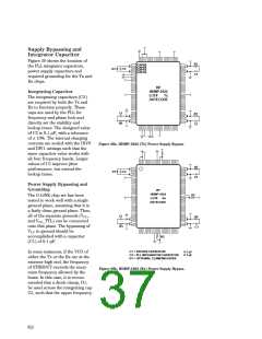
Data Interface for Single/
Double Frame Mode.
transition. Therefore, it is
recommended that the flag bit be
reserved for error detection. With
FLAGSEL disabled, the flag bit is
toggled internally by the Tx, and
the Rx uses this strict alternation
to detect errors, thus making the
link much more reliable.
G-LINK is designed to work with
single frame or double frame
modes, in either 16 or 20 bits
wide per frame. An extra flag bit
is available with FLAGSEL and it
is used to signify the first or
second frames in double- frame
mode. The 16/20 frame width
option is selected with the
M20SEL pin. In this discussion, a
20 bit width is assumed. In both
single and double frame modes,
the data frame (D0-D19), flag bit
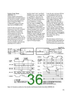
The lock up time in this simplex
configuration is dependent on the
frequency match between the two
local oscillators. This method
relies on a slight difference
Simplex Method III: Simplex
with Reference Oscillator
A third configuration for simplex
operation is shown in Figure 17c.
649

 AGILENT [ AGILENT TECHNOLOGIES, LTD. ]