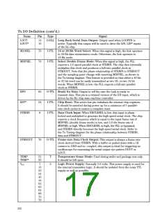
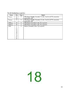
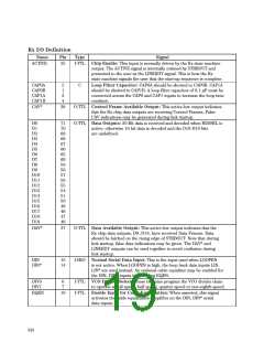
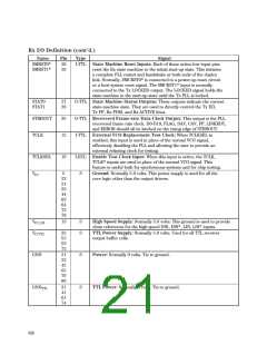
Rx I/O Definition (cont’d.)
Name
Pin
Type
Signal
SMRST0*
SMRST1*
28
29
I-TTL State Machine Reset Inputs: Each of these active-low input pins
reset the Rx state machine to the initial start-up state. This initiates
a complete PLL restart and handshake at both ends of the duplex
link. Normally, SMCRST0* is connected to a power-up reset circuit
or a host system reset signal. The SMCRST1* input is normally
connected to the Tx LOCKED output. The LOCKED signal holds the
state-machine in the start-up state until the Tx PLL is locked.
STAT0
STAT1
27
26
O-TTL State Machine Status Outputs: These outputs indicate the current
state-machine state. They are used to directly control the Tx ED,
Tx FF, Rx FDIS, and Rx ACTIVE lines.
STRBOUT
TCLK
35
12
O-TTL Recovered Frame-rate Data Clock Output: This output is the PLL
recovered frame rate clock. D0-D19, FLAG, DAV, CAV, FF, LINKRDY,
and ERROR should all be latched on the rising edge of STRBOUT.
I-TTL External VCO Replacement Test Clock: When TCLKSEL in
enabled, this input is used in place of the normal VCO signal,
effectively disabling the PLL and allowing the user to provide an
external retiming clock for testing.
TCLKSEL
VCC
10
I-ECL Enable Test Clock Input: When this input is active, the TCLK,
TCLK* inputs are used in place of the normal VCO signal. This
feature is useful both for synchronous systems and for chip testing.
5
S
Ground: Normally 5.0 volts. This power supply is used for all the
23
24
33
44
63
64
73
78
core logic other than the output drivers.
VCC_HS
VCCTTL
13
S
S
High Speed Supply: Normally 5.0 volts. This ground is used to provide
clean references for the high speed DIN, DIN*, LIN, LIN* inputs.
TTL Power Supply: Normally 5.0 volts. Used for all TTL receiver
output buffer cells.
32
52
53
72
GND
21
22
42
62
79
80
31
41
61
74
S
S
Power: Normally 0 volts. Tie to ground.
GNDTTL
TTL Power: Normally 0 volts. Tie to ground.
636

 AGILENT [ AGILENT TECHNOLOGIES, LTD. ]