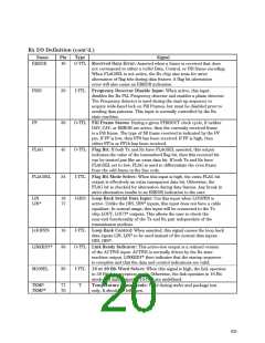
Rx I/O Definition (cont’d.)
Name
Pin
Type
Signal
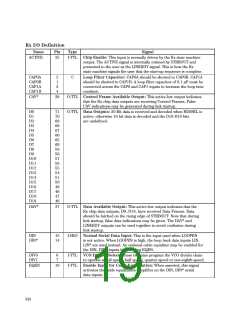
ERROR
40
O-TTL Received Data Error: Asserted when a frame is received that does
not correspond to either a valid Data, Control, or Fill frame encoding.
When FLAGSEL is not active, the Rx chip also tests for strict
alternation of flag bits during data frames. A flag bit alternation
error will also cause an ERROR indication.
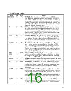
FDIS
20
I-TTL Frequency Detector Disable Input: When active, this input
disables the Rx PLL Frequency detector and enables a phase detector.
The Frequency detector is used during the start-up sequence to
acquire wide-band lock on Fill Frames, but must be disabled prior to
sending data patterns. This input is normally controlled by the Rx
state machine.
FF
39
45
34
O-TTL Fill Frame Status: During a given STRBOUT clock cycle, if neither
DAV, CAV, or ERROR are active, then the currently received frame
is a Fill frame. The type of fill frame received is indicated by the FF
pin. If FF is low, then FF0 has been received. If FF is high, then
either FF1a or FF1b has been received.
O-TTL Flag Bit: If both Tx and Rx have FLAGSEL asserted, this output
indicates the value of the transmitted flag bit, then this received bit
can be treated just like an extra data bit. If both Tx and Rx have
FLAGSEL set to low, FLAG is used to differentiate the even frame
from the odd frame in the line code.
FLAG
FLAGSEL
I-TTL Flag Bit Mode Select: When this input is high, the extra FLAG bit
output is effectively an extra transparent data bit. Otherwise, the
FLAG bit is checked for alternation during data frames. Any break in
strict alternation results in an ERROR indication to the user.
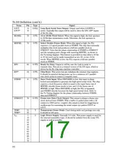
LIN
LIN*
18
17
I-H50 Loop Back Serial Data Input: Use this input when LOOPEN is
active. Unlike the DIN, DIN* inputs, this input does not have a cable
equalizer. In normal usage, this input will be connected to the Tx
chip LOUT, LOUT* outputs. This allows the user to check the
near-end functionality of the Tx and Rx pair independent of the
transmission medium.
LOOPEN
16
36
I-TTL Loop Back Control: When asserted, this signal causes the loop back
data inputs LIN, LIN* to be used instead of the normal data inputs
DIN, DIN*.
O-TTL Link Ready Indicator: This active-low output is a retimed version
of the ACTIVE input. ACTIVE is normally driven by the Rx state
machine output. LINKRDY* then indicates that the startup sequence
is complete and that the data and control indications are valid.
LINKRDY*
M20SEL
30
I-TTL 16 or 20 Bit Word Select: When this signal is high, the link operates
in 20 Bit data reception mode. Otherwise, the link operates in 16 Bit
mode and data outputs D16-D19 are undefined.
TEMP
TEMP*
77
76
T
Temperature Sense Diode: Used during wafer and package test
only. It should be left open.
635

 AGILENT [ AGILENT TECHNOLOGIES, LTD. ]