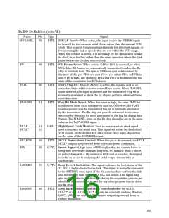
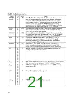
Tx I/O Definition (cont’d.)
Name
LOUT
LOUT*
Pin
Type
Signal
14
15
O-BLL Loop Back Serial Data Output: Output used when LOOPEN is
active. Typically this output will be used to drive the LIN, LIN* inputs
of the Rx chip.
M20SEL
73
74
I-TTL 16 or 20 Bit Word Select: When this signal is high, the link operates
in 20 Bit data transmission mode. Otherwise, the link operates in
16 Bit mode.
MDFSEL
I-TTL Select Double Frame Mode: When this signal is high, the PLL
expects a 1/2 speed parallel clock at STRBIN. The chip then internally
multiplies this clock and produces a full-rate parallel clock at
STRBOUT. Note that the phase relationship of STRBIN to STRBOUT
and the sampling point change with asserting MDFSEL, as shown in
the Tx timing diagram. This feature is provided so that either a 40 bit
or 32 bit word can be easily transmitted as two 20, or two 16 bit
words. When MDFSEL is low, the PLL expects a full-rate parallel
clock at STRBIN.
RFD
65
34
8
O-TTL Ready for Data: Output to tell the user the Link is ready to
transmit data. This pin is a retimed version of the ED input, which is
driven by the Rx chip state machine controller.
RST*
I-TTL Chip Reset: This active-low pin initializes the internal chip registers.
It should be asserted during power up for a minimum of 5 parallel-
rate clock cycles to ensure a complete reset.
STRBIN
I-TTL Data Clock Input: When EHCLKSEL is low, this input is phase
locked and multiplied to generate the high speed serial clock. The chip
expects a clock frequency which is equal to the input frame rate if
MDFSEL (double frame mode) is low, and 1/2 the frame rate if
MDFSEL is high. When EHCLKSEL is high, the PLL is bypassed,
and STRBIN directly becomes the high speed serial clock. Refer to
the Tx Timing diagram for the phase relationship between STRBIN,
data and STRBOUT.
STRBOUT
76
O-TTL Frame-rate Data Clock Output: This output is always a frame rate
clock derived from STRBIN. With a buffer or pulled down with a 1K
resistor to GND and ac- coupled, this output is ideal for triggering an
oscilloscope for examining the serial output eye pattern DOUT or
LOUT.
TEMP
TEMP*
31
32
T
Temperature Sense Diode: Used during wafer and package test only .
It should be left open.
VCC
7
S
Logic Power Supply: Normally 5.0 volts. This power supply is used for
the internal transmitter logic. It should be isolated from the noisy TTL
supply as well as possible.
13
23
24
43
44
52
63
64
66
72
79
632

 AGILENT [ AGILENT TECHNOLOGIES, LTD. ]