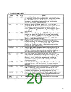
Tx I/O Definition (cont’d.)
Name
Pin
Type
Signal
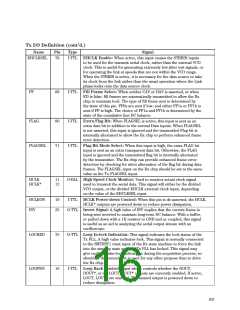
EHCLKSEL
78
I-TTL EHCLK Enable: When active, this input causes the STRBIN inputs
to be used for the transmit serial clock, rather than the internal VCO
clock. This is useful for generating extremely low jitter test signals, or
for operating the link at speeds that are not within the VCO range.
When the STRBIN is active, it is necessary for the data source to take
its clock from the link rather than the usual operation where the Link
phase-locks onto the data source clock.
FF
68
I-TTL Fill Frame Select: When neither CAV or DAV is asserted, or when
ED is false, fill frames are automatically transmitted to allow the Rx
chip to maintain lock. The type of fill frame sent is determined by
the state of this pin. FF0s are sent if low, and either FF1a or FF1b is
sent if FF is high. The choice of FF1a and FF1b is determined by the
state of the cumulative line DC balance.
FLAG
60
71
I-TTL Extra Flag Bit: When FLAGSEL is active, this input is sent as an
extra data bit in addition to the normal Data inputs. When FLAGSEL
is not asserted, this input is ignored and the transmitted Flag bit is
internally alternated to allow the Rx chip to perform enhanced frame
error detection.
FLAGSEL
I-TTL Flag Bit Mode Select: When this input is high, the extra FLAG bit
input is sent as an extra transparent data bit. Otherwise, the FLAG
input is ignored and the transmitted flag bit is internally alternated
by the transmitter. The Rx chip can provide enhanced frame error
detection by checking for strict alternation of the flag bit during data
frames. The FLAGSEL input on the Rx chip should be set to the same
value as the Tx FLAGSEL input.
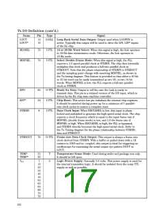
HCLK
HCLK*
11
12
O-BLL High Speed Clock Monitor: Used to monitor actual clock signal
used to transmit the serial data. This signal will either be the divided
VCO output, or the divided EHCLK external clock input, depending
on the value of the EHCLKSEL input.
HCLKON
INV
10
25
I-TTL HCLK Power-down Control: When this pin is de-asserted, the HCLK,
HCLK* outputs are powered down to reduce power dissipation.
O-TTL Invert Signal: A high value of INV implies that the current frame is
being sent inverted to maintain long-term DC balance. With a buffer,
or pulled down with a 1K resistor to GND and ac coupled, this signal
is useful as an aid to analyzing the serial output stream with an
oscilloscope.
LOCKED
LOOPEN
75
16
O-TTL Loop In-lock Indication: This signal indicates the lock status of the
Tx PLL. A high value indicates lock. This signal is normally connected
to the SMTRST1 reset input of the Rx state machine to force the link
into the start-up state until the Tx PLL has locked. This signal may
give multiple false-lock indications during the acquisition process, so
should be debounced if it is used for any other purpose than to drive
the Rx chip.
I-TTL Loop Back Control: Input which controls whether the DOUT,
DOUT*, or the LOUT, LOUT* outputs are currently enabled. If active,
LOUT, LOUT* are enabled. The unused output is powered down to
reduce dissipation.
631

 AGILENT [ AGILENT TECHNOLOGIES, LTD. ]