Ambassador T8100A, T8102, and T8105
H.100/H.110 Interfaces and Time-Slot Interchangers
Advance Data Sheet
November 1999
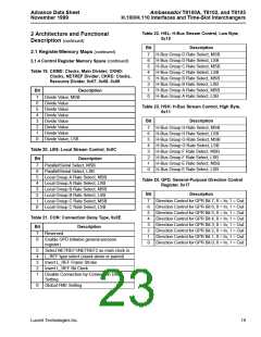
Table 27. FRHA: Frame Group A, High Address and
Control, 0x21
2 Architecture and Functional
Description (continued)
Bit
Description
2.1 Register/Memory Maps (continued)
7
6
5
4
3
2
Rate Select, MSB
Rate Select, LSB
2.1.4 Control Register Memory Space (continued)
Pulse Width Select, MSB
Table 25. GPR: General-Purpose I/O Register, 0x18
Pulse Width Select, LSB
Frame Invert, or Programmed Output, Bit 11
Bit
Description
General-Purpose I/O, MSB
Start Address, MSB, or Programmed Output,
Bit 10
7
6
5
4
3
2
1
0
General-Purpose I/O
General-Purpose I/O
General-Purpose I/O
General-Purpose I/O
General-Purpose I/O
General-Purpose I/O
General-Purpose I/O, LSB
1
0
Start Address, Bit 9, or Programmed Output,
Bit 9
Start Address, Bit 8, or Programmed Output,
Bit 8
Table 28. FRLB: Frame Group B, Start Address
Low, 0x22
Bit
Description
Start Address, Bit 7
Table 26. FRLA: Frame Group A, Start Address
Low, 0x20
7
6
5
4
3
2
1
0
Start Address, Bit 6
Start Address, Bit 5
Start Address, Bit 4
Start Address, Bit 3
Start Address, Bit 2
Start Address, Bit 1
Start Address, LSB
Bit
Description
7
Start Address, Bit 7, or Programmed Output,
Bit 7
6
5
4
3
2
1
0
Start Address, Bit 6, or Programmed Output,
Bit 6
Start Address, Bit 5, or Programmed Output,
Bit 5
Start Address, Bit 4, or Programmed Output,
Bit 4
Table 29. FRHB: Frame Group B, High Address and
Control, 0x23
Start Address, Bit 3, or Programmed Output,
Bit 3
Bit
Description
7
6
5
4
3
2
1
0
Rate Select, MSB
Rate Select, LSB
Start Address, Bit 2, or Programmed Output,
Bit 2
Start Address, Bit 1, or Programmed Output,
Bit 1
Pulse Width Select, MSB
Pulse Width Select, LSB
Frame Inversion Select
Start Address, MSB
Start Address, LSB, or Programmed Output,
Bit 0
Start Address, Bit 9
Start Address, Bit 8
20
Lucent Technologies Inc.

 AGERE [ AGERE SYSTEMS ]