Ambassador T8100A, T8102, and T8105
H.100/H.110 Interfaces and Time-Slot Interchangers
Advance Data Sheet
November 1999
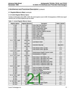
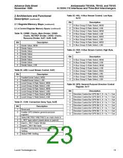
Table 22. HSL: H-Bus Stream Control, Low Byte,
0x10
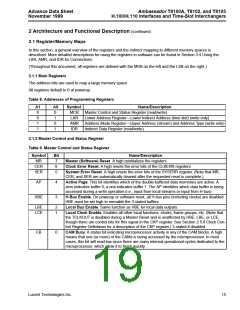
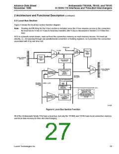
2 Architecture and Functional
Description (continued)
Bit
Description
2.1 Register/Memory Maps (continued)
7
6
5
4
3
2
1
0
H-Bus Group D Rate Select, MSB
H-Bus Group D Rate Select, LSB
H-Bus Group C Rate Select, MSB
H-Bus Group C Rate Select, LSB
H-Bus Group B Rate Select, MSB
H-Bus Group B Rate Select, LSB
H-Bus Group A Rate Select, MSB
H-Bus Group A Rate Select, LSB
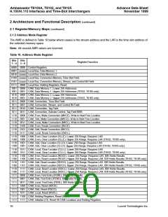
2.1.4 Control Register Memory Space (continued)
Table 19. CKMD: Clocks, Main Divider; CKND:
Clocks, NETREF Divider; CKRD: Clocks,
Resource Divider, 0x07, 0x08, 0x09
Bit
Description
Divide Value, MSB
7
6
5
4
3
2
1
0
Divide Value
Divide Value
Divide Value
Divide Value
Divide Value
Divide Value
Divide Value, LSB
Table 23. HSH: H-Bus Stream Control, High Byte,
0x11
Bit
Description
7
6
5
4
3
2
1
0
H-Bus Group H Rate Select, MSB
H-Bus Group H Rate Select, LSB
H-Bus Group G Rate Select, MSB
H-Bus Group G Rate Select, LSB
H-Bus Group F Rate Select, MSB
H-Bus Group F Rate Select, LSB
H-Bus Group E Rate Select, MSB
H-Bus Group E Rate Select, LSB
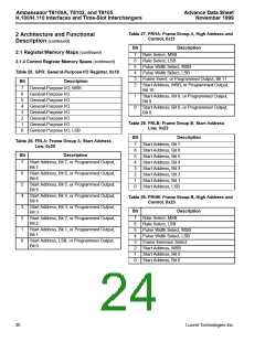
Table 20. LBS: Local Stream Control, 0x0C
Bit
Description
Parallel/Serial Select, MSB
7
6
5
4
3
2
1
0
Parallel/Serial Select, LSB
Local Group A Rate Select, MSB
Local Group A Rate Select, LSB
Local Group B Rate Select, MSB
Local Group B Rate Select, LSB
Local Group C Rate Select, MSB
Local Group C Rate Select, LSB
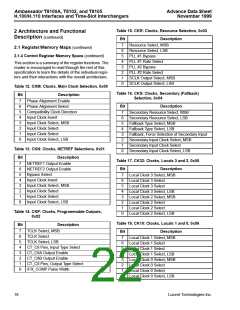
Table 24. GPD, General-Purpose Direction Control
Register, 0x17
Bit
Description
7
6
5
4
3
2
1
0
Direction Control for GPR Bit 7, 0 = In; 1 = Out.
Direction Control for GPR Bit 6, 0 = In; 1 = Out.
Direction Control for GPR Bit 5, 0 = In; 1 = Out.
Direction Control for GPR Bit 4, 0 = In; 1 = Out.
Direction Control for GPR Bit 3, 0 = In; 1 = Out.
Direction Control for GPR Bit 2, 0 = In; 1 = Out.
Direction Control for GPR Bit 1, 0 = In; 1 = Out.
Direction Control for GPR Bit 0, 0 = In; 1 = Out.
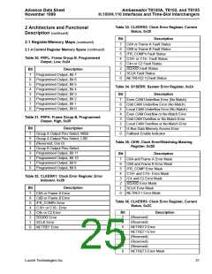
Table 21. CON: Connection Delay Type, 0x0E
Bit
Description
7
6
Reserved
Enable GPD (bitwise general-purpose
register)
5
4
3
2
1
Select NETREF1/NETREF2 as main clock in.
L_REF type select (stand-alone or paired)
Invert L_REF Frame Strobe
Invert L_REF Bit Clock
Disable Connection-by-Connection Delay
Setting
0
Global FME Setting
Lucent Technologies Inc.
19

 AGERE [ AGERE SYSTEMS ]