Ambassador T8100A, T8102, and T8105
H.100/H.110 Interfaces and Time-Slot Interchangers
Advance Data Sheet
November 1999
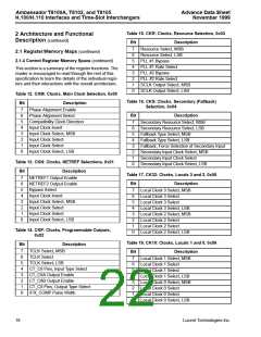
Table 15. CKR: Clocks, Resource Selection, 0x03
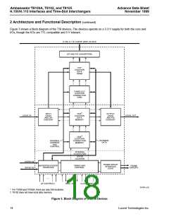
2 Architecture and Functional
Description (continued)
Bit
Description
Resource Select, MSB
7
6
5
4
3
2
1
0
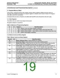
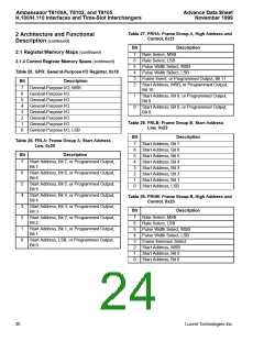
2.1 Register/Memory Maps (continued)
Resource Select, LSB
PLL #1 Bypass
2.1.4 Control Register Memory Space (continued)
PLL #1 Rate Select
PLL #2 Bypass
This section is a summary of the register functions. The
reader is encouraged to read through the rest of this
specification to learn the details of the individual regis-
ters and their interactions with the overall architecture.
PLL #2 Rate Select
SCLK Output Select, MSB
SCLK Output Select, LSB
Table 12. CKM: Clocks, Main Clock Selection, 0x00
Table 16. CKS: Clocks, Secondary (Fallback)
Selection, 0x04
Bit
Description
Phase Alignment Enable
7
6
5
4
3
2
1
0
Bit
Description
Phase Alignment Select
Compatibility Clock Direction
Input Clock Invert
7
6
5
4
3
2
1
0
Secondary Resource Select, MSB
Secondary Resource Select, LSB
Fallback Type Select, MSB
Input Clock Select, MSB
Input Clock Select
Fallback Type Select, LSB
Input Clock Select
Fallback, Force Selection of Secondary Input
Secondary Input Clock Select, MSB
Secondary Input Clock Select
Input Clock Select, LSB
Table 13. CKN: Clocks, NETREF Selections, 0x01
Secondary Input Clock Select, LSB
Bit
Description
NETREF1 Output Enable
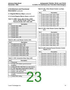
Table 17. CK32: Clocks, Locals 3 and 2, 0x05
7
6
5
4
3
2
1
0
Bit
Description
Local Clock 3 Select, MSB
NETREF2 Output Enable
Bypass Select
7
6
5
4
3
2
1
0
Input Clock Invert
Local Clock 3 Select
Input Clock Select, MSB
Input Clock Select
Local Clock 3 Select
Local Clock 3 Select, LSB
Local Clock 2 Select, MSB
Local Clock 2 Select
Input Clock Select
Input Clock Select, LSB
Local Clock 2 Select
Table 14. CKP: Clocks, Programmable Outputs,
0x02
Local Clock 2 Select, LSB
Table 18. CK10: Clocks, Locals 1 and 0, 0x06
Bit
Description
TCLK Select, MSB
7
6
5
4
3
2
1
0
Bit
Description
Local Clock 1 Select, MSB
TCLK Select
7
6
5
4
3
2
1
0
TCLK Select, LSB
Local Clock 1 Select
CT_C8 Pins, Input Type Select
CT_C8A Output Enable
CT_C8B Output Enable
CT_C8 Pins, Output Type Select
/FR_COMP Pulse Width
Local Clock 1 Select
Local Clock 1 Select, LSB
Local Clock 0 Select, MSB
Local Clock 0 Select
Local Clock 0 Select
Local Clock 0 Select, LSB
18
Lucent Technologies Inc.

 AGERE [ AGERE SYSTEMS ]