Ambassador T8100A, T8102, and T8105
H.100/H.110 Interfaces and Time-Slot Interchangers
Advance Data Sheet
November 1999
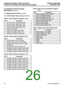
Table 40. DEV_ID: Device Identification Register,
0xFE
2 Architecture and Functional
Description (continued)
Bit
Description
2.1 Register/Memory Maps (continued)
7
6
5
4
3
2
1
0
Device Identification Number, MSB
Device Identification Number
Device Identification Number
Device Identification Number, LSB
Device Version Number, MSB
Device Version Number
2.1.4 Control Register Memory Space (continued)
Table 37. DIAG1: Diagnostics Register 1, 0x30
Bit
Description
7
6
5
4
3
2
1
0
Frame Group A Output Select, MSB
Frame Group A Output Select, LSB
Frame Group B Output Select, MSB
Frame Group B Output Select, LSB
Memory Fill Enable
Device Version Number
Device Version Number, LSB
Table 41. GMODE: Global Mode Register, 0xFF
Bit
Description
Memory Fill Pattern Select, MSB
Memory Fill Pattern Select, LSB
Memory Fill Status Bit (Read Only)
7
6
5
4
3
2
1
0
Mode Emulation Set 2 (ME2)
Mode Emulation Set 1 (ME1)
Subrate Enable (SE)
(Reserved)
Table 38. DIAG2: Diagnostics Register 2, 0x31
EMUL, MSB
Bit
Description
EMUL
7
6
5
4
3
2
1
0
Frame Groups Cycle Test Enable
Break State Counter into Subsections
Bypass Internal Frame with /FR_COMPn
(Reserved)
EMUL
EMUL, LSB
Enable State Counter Parallel Load
Parallel Load Value of State Counter, MSB
Parallel Load Value of State Counter, Bit 9
Parallel Load Value of State Counter, Bit 8
Table 39. DIAG3: Diagnostics Register 3, 0x32
Bit
Description
7
6
5
4
3
2
1
0
Parallel Load Value of State Counter, Bit 7
Parallel Load Value of State Counter, Bit 6
Parallel Load Value of State Counter, Bit 5
Parallel Load Value of State Counter, Bit 4
Parallel Load Value of State Counter, Bit 3
Parallel Load Value of State Counter, Bit 2
Parallel Load Value of State Counter, Bit 1
Parallel Load Value of State Counter, LSB
22
Lucent Technologies Inc.

 AGERE [ AGERE SYSTEMS ]