Ambassador T8100A, T8102, and T8105
H.100/H.110 Interfaces and Time-Slot Interchangers
Advance Data Sheet
November 1999
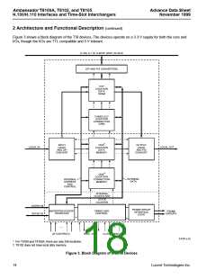
2 Architecture and Functional Description (continued)
2.1 Register/Memory Maps (continued)
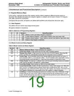
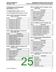
2.1.4 Control Register Memory Space
Function of LAR values when AMR = 0x00. All control registers reset to 0x00. All designations of MSB (most signif-
icant bit) and LSB (least significant bit) are shown.
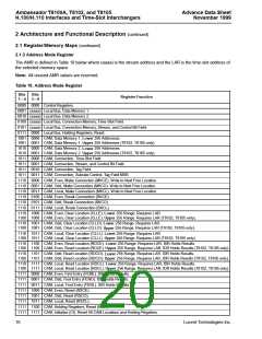
Table 11. Control Register Memory Space
Register Address
Register Mnemonic
Description
Refer to Section
0, 0x00
1, 0x01
CKM
CKN
Clocks, Main Clock Selections
Clocks, NETREF Selections
Clocks, Programmable Outputs
Clocks, Resource Selection
Clocks, Secondary (Fallback) Selection
Clocks, Locals 3 and 2
2.5.8
2.5.8
2.5.8
2.5.8
2.5.8
2.5.8
2.5.8
2.5.8
2.5.8
2.5.8
—
2, 0x02
CKP
3, 0x03
CKR
4, 0x04
CKS
5, 0x05
CK32
6, 0x06
CK10
Clocks, Locals 1 and 0
7, 0x07
CKMD
Clocks, Main Divider
8, 0x08
CKND
Clocks, NETREF Divider
Clocks, Resource Divider
—
9, 0x09
CKRD
10—11, 0x0A—0x0B
12, 0x0C
(Reserved)
LBS
Local Stream Control
2.2.4
—
13, 0x0D
(Reserved)
CON
—
14, 0x0E
Connection Delay Type
—
Appendix B
—
15, 0x0F
(Reserved)
HSL
16, 0x10
H-Bus Stream Control, Low Byte
H-Bus Stream Control, High Byte
—
2.3.5
2.3.5
—
17, 0x11
HSH
18—22, 0x12—0x16
23, 0x17
(Reserved)
GPD
General-purpose Register, Direction Control
General-purpose I/O Register
—
2.6.2
2.6.2
—
24, 0x18
GPR
25—31, 0x19—0x1F
32, 0x20
(Reserved)
FRLA
Frame Group A, Start Address, Low
Frame Group A, High Address and Control
Frame Group B, Start Address, Low
Frame Group B, High Address and Control
Frame Group B, Programmed Output, Low
Frame Group B, Programmed Output, High
—
2.6.3
2.6.3
2.6.3
2.6.3
2.6.3
2.6.3
—
33, 0x21
FRHA
34, 0x22
FRLB
35, 0x23
FRHB
36, 0x24
FRPL
37, 0x25
FRPH
38—39, 0x26—0x27
40, 0x28
(Reserved)
CLKERR1
CLKERR2
SYSERR
CKW
Clock Error Register, Error Indicator
Clock Error Register, Current Status
System Error Register
2.7
41, 0x29
2.7
42, 0x2A
2.7
43, 0x2B
Clock Error/Watchdog Masking Register
Clock Error Register, Current Status
—
2.5.7 & 2.7
2.7
44, 0x2C
CLKERR3
(Reserved)
DIAG1
DIAG2
DIAG3
(Reserved)
DEV_ID
GMODE
45—47, 0x2D—0x2F
48, 0x30
—
Diagnostics Register 1
2.9.2
2.9.2
2.9.2
—
49, 0x31
Diagnostics Register 2
50, 0x32
Diagnostics Register 3
51—253, 0x33—0xFD
254, 0xFE
255, 0xFF
—
Device Revision Status Register
Global Mode Register
3.2.1
3.2.1
Lucent Technologies Inc.
17

 AGERE [ AGERE SYSTEMS ]