Ambassador T8100A, T8102, and T8105
H.100/H.110 Interfaces and Time-Slot Interchangers
Advance Data Sheet
November 1999
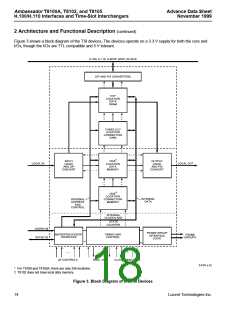
2 Architecture and Functional Description (continued)
2.1 Register/Memory Maps
In this section, a general overview of the registers and the indirect mapping to different memory spaces is
described. More detailed descriptions for using the registers in software can be found in Section 3.4 Using the
LAR, AMR, and IDR for Connections.
(Throughout this document, all registers are defined with the MSB on the left and the LSB on the right.)
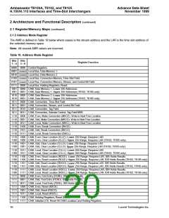
2.1.1 Main Registers
The address bits are used to map a large memory space.
All registers default to 0 at powerup.
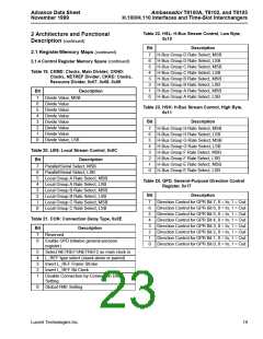
Table 8. Addresses of Programming Registers
A1
0
A0
0
Symbol
MCR
LAR
Name/Description
Master Control and Status Register (read/write)
0
1
Lower Address Register—Lower Indirect Address (time slot) (write only)
Address Mode Register—Upper Address (stream) and Address Type (write only)
Indirect Data Register (read/write)
1
0
AMR
IDR
1
1
2.1.2 Master Control and Status Register
Table 9. Master Control and Status Register
Symbol
MR
Bit
7
Name/Description
Master (Software) Reset. A high reinitializes the registers.
Clock Error Reset. A high resets the error bits of the CLKERR registers.
CER
6
SER
5
System Error Reset. A high resets the error bits of the SYSERR register. (Note that MR,
CER, and SER are automatically cleared after the requested reset is complete.)
AP
4
3
Active Page. This bit identifies which of the double-buffered data memories are active. A
zero indicates buffer 0; a one indicates buffer 1. The AP identifies which data buffer is being
accessed during a write operation (i.e., input from local streams or input from H-bus).
HBE
H-Bus Enable. On powerup or software reset, all H-bus pins (including clocks) are disabled.
HBE must be set high to reenable the 3-stated buffers.
LBE
LCE
2
1
Local Bus Enable. Same function as HBE for local data outputs.
Local Clock Enable. Enables all other local functions: clocks, frame groups, etc. (Note that
the TCLKOUT is disabled during a Master Reset and is unaffected by HBE, LBE, or LCE,
though there are control bits for this signal in the CKP register. See Section 2.5.8 Clock Con-
trol Register Definitions for a description of the CKP register.) 3-stated if disabled.
CB
0
CAM Busy. A status bit indicating microprocessor activity in any of the CAM blocks. A high
means that one (or more) of the CAMs is being accessed by the microprocessor. In most
cases, this bit will read low since there are many internal operational cycles dedicated to the
microprocessor, which allow it to finish quickly.
Lucent Technologies Inc.
15

 AGERE [ AGERE SYSTEMS ]