Ambassador T8100A, T8102, and T8105
H.100/H.110 Interfaces and Time-Slot Interchangers
Advance Data Sheet
November 1999
1 Product Overview (continued)
1.3 Pin Information (continued)
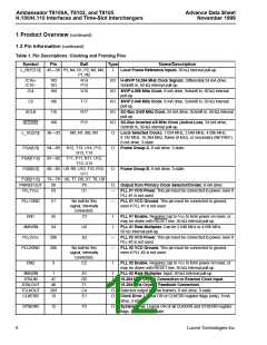
Table 6. Pin Descriptions: Power Pins
Symbol
Pin
Ball
Type
Name/Description
VSS
11, 23, 37, 49, 57,
72, 86, 100, 103,
B2, B16, C3, C15,
D4, D9, D14, H8,
—
Chip Ground.
105, 109, 111, 117, H9, H10, J4, J8, J9,
119, 121, 127, 138, J10, J14, K8, K9,
143, 153, 163, 173, K10, L15, N14, P4,
184, 204
P9, P14, P16, R3,
R15, T2, T15, T16,
U15, U17
VDD
14, 32, 46, 63, 79,
93, 107, 124, 132,
148, 158, 168, 178,
193
A16, D8, D10, F2,
H4, H14, K4, K14,
L16, P8, P10, T9
—
3.3 V Supply Voltage. Decouple every VDD pin
with a 0.1 µF ceramic capacitor to VSS. 1000 pF or
0.01 µF capacitors may be used in addition to the
0.1 µF capacitor to provide additional decoupling.
Place the capacitor as close to the VDD pin as pos-
sible.
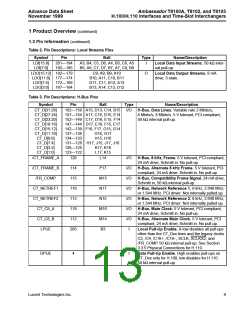
Table 7. Pin Descriptions: Other Pins
Symbol
Pin
Ball
Type
Name/Description
GP[5:0]
66—71
T5, R6, U5, T6,
R7, P7
I/O General-Purpose Bidirectional Register. 8 mA
drive, Schmitt in, 50 kΩ internal pull-up.
TODJAT/GP6
65
64
U4
I/O Output from Selector to Drive DJAT (for
NETREF) or GP Register Bit 6.
8 mA drive, Schmitt in, 50 kΩ internal pull-up.
FROMDJAT/GP7
R5
I/O Smoothed Input to NETREF Divider and Driv-
ers or GP Register Bit 7.
8 mA drive, input, Schmitt in, 50 kΩ internal pull-
up.
XCS
TTS
(NC)
183
10
A8
D1
O
I
Serial Output from Connection Memory. 8 mA
drive, 3-state.
Test Type Select. 0 = JTAG, 1 = forced output
test, internal pull-down.
2, 50, 52,
56, 59, 60,
A12, B1, B14, B17,
C12, D5, E2, J2,
—
Reserved, No Connection.
61, 62, 135, L3, M17, N16, P6,
202, 207 R4, R16, T4, U3
Lucent Technologies Inc.
11

 AGERE [ AGERE SYSTEMS ]