Data Sheet
AD5940
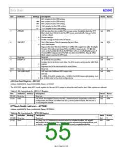
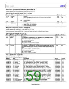
Repeat ADC Conversions Control Register—REPEATADCCNV
Address 0x000021F0, Reset: 0x00000160, Name: REPEATADCCNV
Table 51. Bit Descriptions for REPEATADCCNV Register
Bits
Bit Name
Reserved
NUM
Settings
Description
Reset
0x0
Access
R
[31:12]
[11:4]
Reserved.
Repeat value. Writing 0 to these bits causes unpredictable operation.
1 conversion.
0x16
R/W
1
0xFF 256 conversions.
Reserved.
[3:1]
0
Reserved
0x0
0x0
R
EN_P enable
Enable repeat ADC conversions.
R/W
0
1
Disable repeat ADC conversions.
Enable repeat ADC conversions.
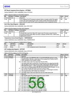
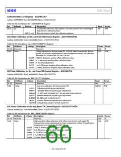
ADC Buffer Configuration Register—ADCBUFCON
Address 0x0000238C, Reset: 0x005F3D00, Name: ADCBUFCON
The recommended value is 0x005F3D0F in high power mode and 0x005F3D04 in low power mode.
Table 52. Bit Descriptions for ADCBUFCON
Bits
[31:9]
[8:4]
Bit Name
Reserved
AMPDIS
Settings
Description
Reserved.
Reset
0x0
Access
R
Set these bits to 1 to disable the op amp. Set these bits to 0 to enable the op amp.
Bit 8 controls the offset cancellation buffers.
Bit 7 controls the ADC buffers.
0x10
R/W
Bit 6 controls the PGA.
Bit 5 controls the positive front-end buffer.
Bit 4 controls the negative front-end buffer.
[3:0]
CHOPDIS
Set these bits to 1 to disable chop. Set these bits to 0 to enable chop. Clear these
0x0
R/W
bits when measuring signals <80 kHz. Set these bits when measuring signals >80
kHz.
Bit 3 controls the offset cancellation buffers.
Bit 2 controls the ADC buffers.
Bit 1 controls the PGA.
Bit 0 controls the front-end buffers.
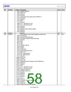
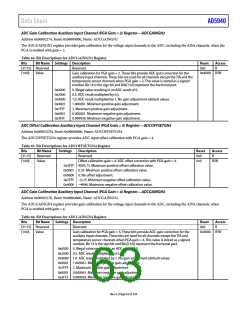
ADC CALIBRATION REGISTERS
Table 53. ADC Calibration Registers Summary
Address
Name
Description
Reset
Access
0x00002230
0x00002288
0x0000228C
0x00002234
0x00002284
0x00002244
0x00002240
0x000022CC
0x00002270
0x000022C8
0x00002274
0x000022D4
0x00002278
0x000022D0
0x00002298
0x0000223C
0x00002238
CALDATLOCK
ADCOFFSETLPTIA
ADCGNLPTIA
ADC calibration lock register
0x00000000
0x00000000
0x00004000
0x00000000
0x00004000
0x00000000
0x00004000
0x00000000
0x00004000
0x00000000
0x00004000
0x00000000
0x00004000
0x00000000
0x00004000
0x00000000
0x00004000
R/W
R/W
R/W
R/W
R/W
R/W
R/W
R/W
R/W
R/W
R/W
R/W
R/W
R/W
R/W
R/W
R/W
ADC offset calibration on the low power TIA channel register
ADC gain calibration for the low power TIA channel register
ADC offset calibration on the high speed TIA channel register
ADC gain calibration for the high speed TIA channel register
ADC offset calibration auxiliary channel (PGA gain = 1) register
ADC gain calibration auxiliary input channel (PGA gain = 1) register
ADC offset calibration auxiliary input channel (PGA gain = 1.5) register
ADC gain calibration auxiliary input channel (PGA gain = 1.5) register
ADC offset calibration auxiliary input channel (PGA gain = 2) register
ADC gain calibration auxiliary input channel (PGA gain = 2) register
ADC offset calibration auxiliary input channel (PGA gain = 4) register
ADC gain calibration auxiliary input channel (PGA gain = 4) register
ADC offset calibration auxiliary input channel (PGA gain = 9) register
ADC gain calibration auxiliary input channel (PGA gain = 9) register
ADC offset calibration temperature sensor channel register
ADC gain calibration temperature sensor channel register
ADCOFFSETHSTIA
ADCGAINHSTIA
ADCOFFSETGN1
ADCGAINGN1
ADCOFFSETGN1P5
ADCGAINGN1P5
ADCOFFSETGN2
ADCGAINGN2
ADCOFFSETGN4
ADCGAINGN4
ADCOFFSETGN9
ADCGAINGN9
ADCOFFSETTEMPSENS
ADCGAINTEMPSENS
Rev. 0 | Page 59 of 130

 ADI [ ADI ]