Data Sheet
AD5940
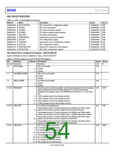
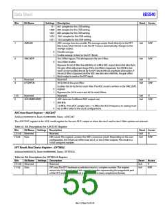
Bits
Bit Name
Settings Description
Reset Access
111 667 samples for this OSR setting.
1000 800 samples for this OSR setting.
1001 889 samples for this OSR setting.
1010 1067 samples for this OSR setting.
1011 1333 samples for this OSR setting.
7
6
AVRGEN
ADC average function enable. The average output feeds directly to the DFT
block and, when this bit is set, the DFT source automatically changes to the
average output.
0x0
0x0
R/W
R/W
0
1
Disable average.
Enable average to feed to the DFT block.
Sinc3 filter bypass. This bit bypasses the sinc3 filter.
Sinc3 filter enable.
SINC3BYP
0
Bypasses the sinc3 filter. Raw 800 kHz or1.6 MHz ADC output data is fed directly to
the gain offset adjustment stage. If the sinc3 filter is bypassed, the 200 kHz sine
wave can be handled directly by the DFT block without amplitude attenuation. If
the sinc3 filter is bypassed and the ADC raw data rate is 800 kHz, the gain offset
block output is used as the DFT input.
1
5
4
Reserved
Reserved
0x0
0x0
R
LPFBYPEN
50 Hz/60 Hz low-pass filter.
R/W
Enables the 50 Hz/60 Hz notch filter. The ADC result is written to the SINC2DAT
register.
Bypasses the 50 Hz notch and 60 Hz notch filters.
0
1
[3:1]
0
Reserved
Reserved.
0x0
0x0
R
ADCSAMPLERATE
ADC data rate. Unfiltered ADC output rate.
800 kHz.
1.6 MHz. If the ADC sample rate = 1.6 MHz, the ACLK frequency to analog must
be 32 MHz (refer to the clock configuration).
R/W
1
0
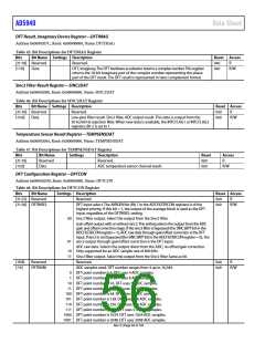
ADC Raw Result Register—ADCDAT
Address 0x00002074, Reset: 0x00000000, Name: ADCDAT
The ADCDAT register is the ADC result register for the raw ADC output or when the sinc3 and/or sinc2 filter options are selected.
Table 43. Bit Descriptions for ADCDAT Register
Bits
[31:16] Reserved
[15:0] Data
Bit Name Settings Description
Reset Access
Reserved.
0x0
0x0
R
ADC result. This register contains the ADC conversion result. Depending on the user
configuration, this result can reflect raw, sinc3, or sinc2 filter outputs. This result is a
16-bit unsigned number.
R/W
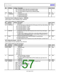
DFT Result, Real Device Register—DFTREAL
Address 0x00002078, Reset: 0x00000000, Name: DFTREAL
Table 44. Bit Descriptions for DFTREAL Register
Bits
[31:18] Reserved
[17:0] Data
Bit Name Settings Description
Reset Access
Reserved.
0x0
0x0
R
DFT, real. The DFT hardware accelerator returns a complex number. This register
returns the 18-bit real part of the complex number representing the magnitude part
of the DFT result. The DFT result is represented in twos complement format.
R/W
Rev. 0 | Page 55 of 130

 ADI [ ADI ]