AD5940
Data Sheet
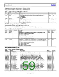
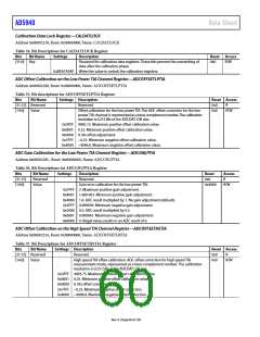
Calibration Data Lock Register—CALDATLOCK
Address 0x00002230, Reset: 0x00000000, Name: CALDATLOCK
Table 54. Bit Descriptions for CALDATLOCK Register
Bits
Bit Name
Settings
Description
Reset Access
[31:0] Key
Password for calibration data registers. These bits prevent the overwriting of
data after the calibration phase.
0x0
R/W
0xDE87A5AF Write this value to unlock the calibration registers.
ADC Offset Calibration on the Low Power TIA Channel Register—ADCOFFSETLPTIA
Address 0x00002288, Reset: 0x00000000, Name: ADCOFFSETLPTIA
Table 55. Bit descriptions for ADCOFFSETLPTIA Register
Bits
[31:15] Reserved
[14:0] Value
Bit Name
Settings Description
Reset Access
Reserved.
0x0
0x0
R
Offset calibration for the low power TIA. The ADC offset correction for the low
R/W
power TIA channel is represented as a twos complement number. The calibration
resolution is 0.25 LSBs of the ADCDAT LSB size.
0x3FFF 4095.75. Maximum positive offset calibration value.
0x0001 0.25. Minimum positive offset calibration value.
0x0000 0. No offset adjustment.
0x7FFF −0.25. Minimum negative offset calibration value.
0x4000 −4096.0. Maximum negative offset calibration value.
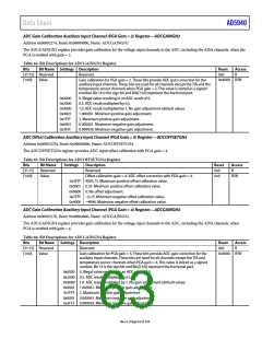
ADC Gain Calibration for the Low Power TIA Channel Register—ADCGNLPTIA
Address 0x0000228C, Reset: 0x00004000, Name: ADCGNLPTIA
Table 56. Bit Descriptions for ADCGNLPTIA Register
Bits
Bit Name
Reserved
Value
Settings
Description
Reset
Access
R
[31:15]
[14:0]
Reserved.
0x0
Gain error calibration for the low power TIA.
0x4000
R/W
0x7FFF 2. Maximum positive gain adjustment.
0x4001 1.000 061. Minimum positive gain adjustment.
0x4000 1.0. ADC result multiplied by 1. No gain adjustment (default).
0x3FFF 0.999939. Minimum negative gain adjustment.
0x2000 0.5. ADC result multiplied by 0.5.
0x0001 0.000061. Maximum negative gain adjustment.
0x0000 0. Illegal value; results in an ADC result of 0.
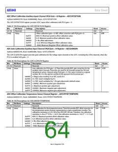
ADC Offset Calibration on the High Speed TIA Channel Register—ADCOFFSETHSTIA
Address 0x00002234, Reset: 0x00000000, Name: ADCOFFSETHSTIA
Table 57. Bit Descriptions for ADCOFFSETHSTIA Register
Bits
[31:15] Reserved
[14:0] Value
Bit Name
Settings Description
Reset Access
Reserved.
0x0
0x0
R
High speed TIA offset calibration. ADC offset correction for high speed TIA
R/W
measurement mode, represented as a twos complement number. The calibration
resolution is 0.25 LSBs of the ADCDAT LSB size.
0x3FFF 4095.75. Maximum positive offset calibration value.
0x0001 0.25. Minimum positive offset calibration value.
0x0000 0. No offset correction.
0x7FFF −0.25. Minimum negative offset correction.
0x4000 −4096.0. Maximum negative offset correction.
Rev. 0 | Page 60 of 130

 ADI [ ADI ]