Data Sheet
AD5940
Bits
Bit Name
Settings Description
Reset Access
1010 DFT point number is 4096. DFT uses 4096 ADC samples.
1011 DFT point number is 8192. DFT uses 8192 ADC samples.
1100 DFT point number is 16,384. DFT uses 16,384 ADC samples.
Reserved.
[3:1]
0
Reserved
0x0
0x0
R
HANNINGEN
Hanning window enable.
R/W
0
1
Disable Hanning window.
Enable Hanning window.
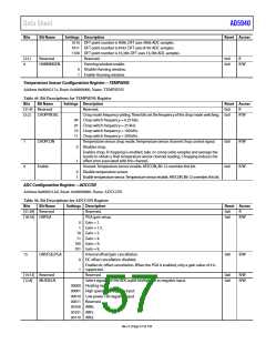
Temperature Sensor Configuration Register—TEMPSENS
Address 0x00002174, Reset: 0x00000000, Name: TEMPSENS
Table 49. Bit Descriptions for TEMPSENS Register
Bits
Bit Name
Settings Description
Reset Access
[31:4] Reserved
Reserved.
0x0
R
[3:2]
CHOPFRESEL
Chop mode frequency setting. These bits set the frequency of the chop mode switching. 0x0
00 Chop switch frequency = 6.25 kHz.
R/W
01 Chop switch frequency = 25 kHz.
10 Chop switch frequency = 100 kHz.
11 Chop switch frequency = 200 kHz.
1
0
CHOPCON
Enable
Temperature sensor chop mode. Temperature sensor channel chop control signal.
Disables chop.
Enables chop. If chopping is enabled, take 2× consecutive samples and average the
results to obtain a final temperature sensor channel reading. Chopping reduces the
offset error associated with this channel.
0x0
0x0
R/W
R/W
0
1
Unused. Temperature sensor enable. AFECON, Bit 12 overrides this bit.
Disable temperature sensor.
Enable temperature sensor. Temperature sensor enable. AFECON, Bit 12 overrides this bit.
0
1
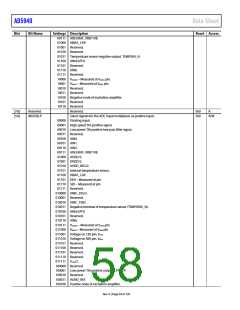
ADC Configuration Register—ADCCON
Address 0x000021A8, Reset: 0x00000000, Name: ADCCON
Table 50. Bit Descriptions for ADCCON Register
Bits
Bit Name
Settings Description
Reset Access
[31:29] Reserved
[18:16] GNPGA
Reserved.
0x0
0x0
R
PGA gain setup.
R/W
0
1
Gain = 1.
Gain = 1.5.
10 Gain = 2.
11 Gain = 4.
100 Gain = 9.
101 Gain = 9.
15
GNOFSELPGA
Internal offset/gain cancellation.
0x0
R/W
0
1
DC offset cancellation disabled.
Enables dc offset cancellation. When the PGA is enabled, only a gain value of 4 is
supported.
[14:13] Reserved
Reserved.
0x0
0x0
R/W
R/W
[12:8]
MUXSELN
Select signals for the ADC input multiplexer as negative input.
00000 Floating input.
00001 High speed TIA negative input
00010 Low power TIA negative input
00011 Reserved.
00100 AIN0.
00101 AIN1.
00110 AIN2.
Rev. 0 | Page 57 of 130

 ADI [ ADI ]