AD5940
Data Sheet
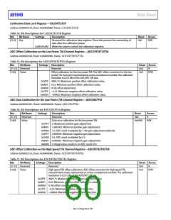
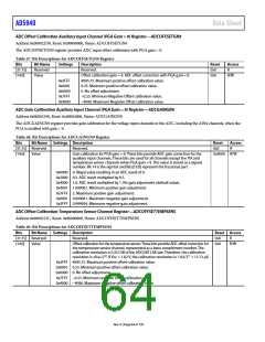
ADC Offset Calibration Auxiliary Input Channel (PGA Gain = 1.5) Register—ADCOFFSETGN1P5
Address 0x000022CC, Reset: 0x00000000, Name: ADCOFFSETGN1P5
The ADCOFFSETGN1P5 register provides ADC input offset calibration with PGA gain =1.5.
Table 61. Bit Descriptions for ADCOFFSETGN1P5 Register
Bits
Bit Name
Reserved
Value
Settings
Description
Reset
0x0
Access
R
[31:15]
[14:0]
Reserved.
Offset calibration gain = 1.5. ADC offset correction with PGA gain = 1.5.
0x0
R/W
0x3FFF 4095.75. Maximum positive offset calibration value.
0x0001 0.25. Minimum positive offset calibration value.
0x0000 0. No offset adjustment.
0x7FFF −0.25. Minimum negative offset calibration value.
0x4000 −4096. Maximum negative offset calibration value.
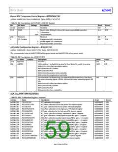
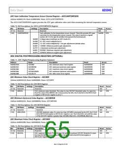
ADC Gain Calibration Auxiliary Input Channel (PGA Gain = 1.5) Register—ADCGAINGN1P5
Address 0x00002270, Reset: 0x00004000, Name: ADCGAINGN1P5
The ADCGAINGN1P5 register provides gain calibration for the voltage input channels to the ADC, including the AINx channels.
Table 62. Bit Descriptions for ADCGAINGN1P5 Register
Bits
[31:15] Reserved
[14:0] Value
Bit Name Settings Description
Reset
Access
Reserved.
0x0
R
Gain calibration for PGA gain = 1.5. These bits provide ADC gain correction for the
auxiliary input channels. These bits are used for all channels except the TIA and
temperature sensor channels when PGA gain =1.5. This value is stored as a signed
number. Bit 14 is the sign bit and Bits[13:0] represent the fractional part.
0x4000 R/W
0x0000 0. Illegal value resulting in an ADC result of 0.
0x2000 0.5. ADC result multiplied by 0.5.
0x4000 1.0. ADC result multiplied by 1. No gain adjustment (default value).
0x4001 1.000061. Minimum positive gain adjustment.
0x7FFF 2. Maximum positive gain adjustment.
0x0001 0.000061. Maximum negative gain adjustment.
0x3FFF 0.999939. Minimum negative gain adjustment.
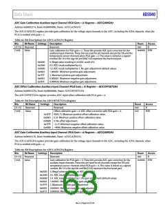
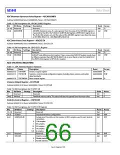
ADC Offset Calibration Auxiliary Input Channel (PGA Gain = 2) Register—ADCOFFSETGN2
Address 0x000022C8, Reset: 0x00000000, Name: ADCOFFSETGN2
The ADCOFFSETGN2 register provides ADC input offset calibration with PGA gain = 2
Table 63. Bit Descriptions for ADCOFFSETGN2 Register
Bits
[31:15] Reserved
[14:0] Value
Bit Name Settings Description
Reset Access
Reserved.
0x0
0x0
R
Offset calibration auxiliary channel (PGA gain = 2). These bits provide ADC offset
correction for inputs using PGA gain = 2, represented as a twos complement number.
The calibration resolution is 0.25 LSB of the ADCDAT LSB size. Therefore, the calibration
resolution is VREF/218. If VREF = 1.82 V, the calibration resolution is 1.8/217 = 13.73 µV.
R/W
0x3FFF 4095.75. Maximum positive offset calibration value.
0x0001 0.25. Minimum positive offset calibration value.
0x0000 0. No offset adjustment.
0x7FFF −0.25. Minimum negative offset calibration value.
0x4000 −4096. Maximum negative offset calibration value.
Rev. 0 | Page 62 of 130

 ADI [ ADI ]