Data Sheet
AD5940
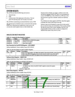
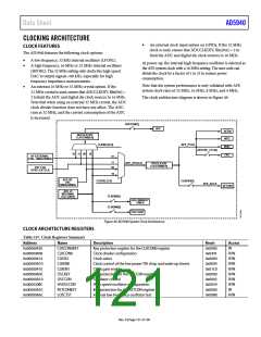
CLOCKING ARCHITECTURE
CLOCK FEATURES
The AD5940 features the following clock options:
An external clock input option on GPIOx. If the 32 MHz
clock is used, ensure that ADCCLKDIV, Bits[9:6] = 2 to
limit the ADC and digital die clock sources to 16 MHz.
A low frequency, 32 kHz internal oscillator (LFOSC).
A high frequency, 16 MHz or 32 MHz internal oscillator
(HFOSC). The 32 MHz setting only clocks the high speed
DAC to output signals >80 kHz, especially for high
frequency impedance measurements.
An external 16 MHz or 32 MHz crystal option. If the
32 MHz crystal is used, ensure that ADCCLKDIV, Bits[9:6] =
2 to limit the ADC and digital die clock sources to 16 MHz.
Note that when using an external 32 MHz crystal, the ADC
clock divider function does not have any affect. The ADC
runs at 32 MHz, and the current consumption of the ADC
is increased.
At power-up, the internal high frequency oscillator is selected as
the AFE system clock with a 16 MHz setting. The user code can
divide the clock by a factor of 1 to 32 to reduce power
consumption.
Note that the system performance is only validated with AFE
system clock rates of 32 MHz, 16 MHz, 8 MHz, and 4 MHz.
The clock architecture diagram is shown in Figure 49.
AFECON[7]
ADC
AFEM
ADCCLK DIV
CLKCON0[9:6]
INTC
AFE_PCLK
MISC
CLKSEL[3:2]
AFECRC_CTL[0]
01 11 00 10
CRC
HF EXTERNAL
XTAL 16MHz/32MHz
01
11
00
AFE_SYSCLK
SYSCLK DIV
CLKCON0[9:6]
EXT CLK
GPIO1 EXTCLK
10
AFE HF
OSC
16MHz/32MHz
CLKSEL[1:0]
CLKEN1[5]
AFE_ACLK
DFT/WG
AFE LF
INTERNAL
OSC 32kHz
CLKEN0[1]
CLKEN0[2]
AFE WAKEUP
TIMER
TIA CHOP
Figure 49. AD5940 System Clock Architecture
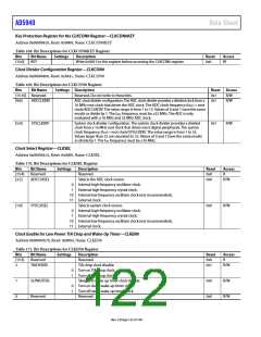
CLOCK ARCHITECTURE REGISTERS
Table 167. Clock Registers Summary
Address
Name
Description
Reset
Access
W
0x00000420
0x00000408
0x00000414
0x00000A70
0x00000410
0x00000A0C
0x00000A10
0x000020BC
0x00000A5C
0x00000A6C
CLKCON0KEY
CLKCON0
CLKSEL
CLKEN0
CLKEN1
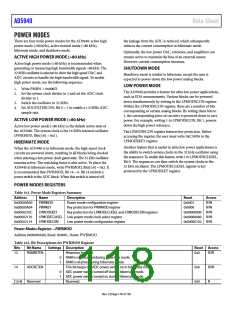
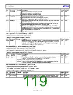
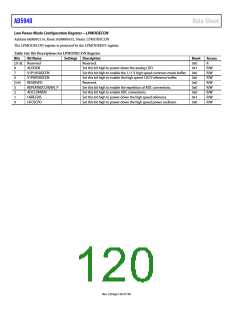
Key protection register for the CLKCON0 register
Clock divider configuration
Clock select
Clock control of the low power TIA chop and wake-up timers
Clock gate enable
Key protection for the OSCCON register
Oscillator control
High speed oscillator configuration
Key protection for the RSTCON register
Internal low frequency oscillator test
0x0000
0x0441
0x0000
0x0004
0x01C0
0x0000
0x0003
0x0034
0x0000
0x0088
R/W
R/W
R/W
R/W
R/W
R/W
R/W
W
OSCKEY
OSCCON
HSOSCCON
RSTCONKEY
LOSCTST
R/W
Rev. 0 | Page 121 of 130

 ADI [ ADI ]