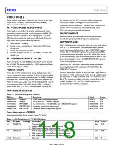
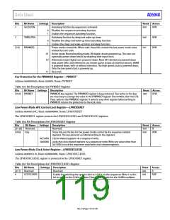
AD5940
Data Sheet
Key Protection Register for the CLKCON0 Register—CLKCON0KEY
Address 0x00000420, Reset: 0x0000, Name: CLKCON0KEY
Table 168. Bit Descriptions for CLKCON0KEY Register
Bits
[15:0]
Bit Name
KEY
Settings
Description
Reset
0x0
Access
W
Write 0xA815 to this register before accessing the CLKCON0 register
Clock Divider Configuration Register—CLKCON0
Address 0x00000408, Reset: 0x0441, Name: CLKCON0
Table 169. Bit Descriptions for CLKCON0 Register
Bits
Bit Name
Settings Description
Reset Access
[15:10] Reserved
Reserved. Do not write to these bits.
0x1
0x1
R/W
R/W
[9:6]
[5:0]
ADCCLKDIV
ADC clock divider configuration. The ADC clock divider provides a divided clock from a
16 MHz root clock that drives the ADC clock. The ADC clock frequency (fADC) = root
clock/ADCCLKDIV. The value range is from 1 to 15. Values of 0 and 1 have the same
results as divide by 1. The fADC frequency must be ≤32 MHz. The ADC is only
evaluated with a 16 MHz and 32 MHz ADC clock.
SYSCLKDIV
System clock divider configuration. The system clock divider provides a divided
clock from a 16 MHz root clock that drives most digital peripherals. The system
clock frequency (fSYS) = root clock/SYSCLKDIV. The value range is from 1 to 32.
Values larger than 32 are saturated to 32. Values of 0 and 1 have the same results
as divide by 1. The fSYS frequency must be ≤16 MHz.
0x1
R/W
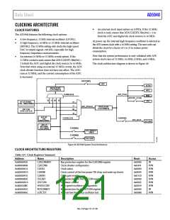
Clock Select Register—CLKSEL
Address 0x00000414, Reset: 0x0000, Name: CLKSEL
Table 170. Bit Descriptions for CLKSEL Register
Bits
[15:4]
[3:2]
Bit Name
Reserved
Settings
Description
Reserved.
Reset
0x0
Access
R
ADCCLKSEL
Selects the ADC clock source.
Internal high frequency oscillator clock.
External high frequency crystal clock.
0x0
R/W
0
1
10 Internal low frequency oscillator clock (not recommended).
11 External clock.
[1:0]
SYSCLKSEL
Selects system clock source.
0x0
R/W
0
1
Internal high frequency oscillator clock.
External high frequency crystal clock.
10 Internal low frequency oscillator clock (not recommended).
11 External clock.
Clock Enable for Low Power TIA Chop and Wake-Up Timer—CLKEN0
Address 0x00000A70, Reset: 0x0004, Name: CLKEN0
Table 171. Bit Descriptions for CLKEN0 Register
Bits
[15:3]
2
Bit Name
Reserved
TIACHSDIS
Settings
Description
Reserved.
Reset
0x0
0x1
Access
R
R/W
TIA chop clock disable.
Turn on TIA chop clock.
Turn off TIA chop clock.
Sleep and wake-up timer clock disable.
Turn on sleep wake-up timer clock.
Turn off sleep wake-up timer clock.
Reserved.
0
1
1
0
SLPWUTDIS
Reserved
0x0
0x0
R/W
R/W
0
1
Rev. 0 | Page 122 of 130

 ADI [ ADI ]