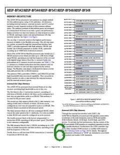
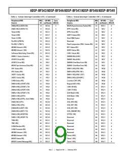
ADSP-BF542/ADSP-BF544/ADSP-BF547/ADSP-BF548/ADSP-BF549
MEMORY ARCHITECTURE
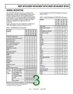
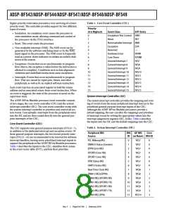
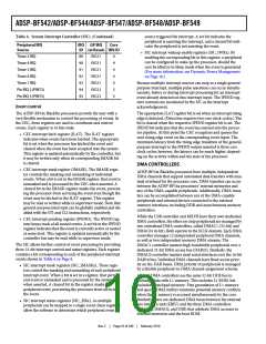
0xFFFF FFFF
The ADSP-BF54x processors view memory as a single unified
CORE MMR REGISTERS (2M BYTES)
4G byte address space, using 32-bit addresses. All resources,
including internal memory, external memory, and I/O control
registers, occupy separate sections of this common address
space. The memory portions of this address space are arranged
in a hierarchical structure to provide a good cost/performance
balance of some very fast, low-latency on-chip memory as cache
or SRAM, and larger, lower-cost and performance off-chip
memory systems. See Figure 3 on Page 6.
0x
FFE0 0000
SYSTEM MMR REGISTERS (2M BYTES)
RESERVED
0xFFC0 0000
0x
FFB0 1000
SCRATCHPAD SRAM (4K BYTES)
RESERVED
0xFFB0 0000
0xFFA2 4000
0xFFA1 4000
L1 ROM (64K BYTE)
INSTRUCTION SRAM / CACHE (16K BYTES)
RESERVED
0x
0x
0x
FFA1 0000
The on-chip L1 memory system is the highest-performance
memory available to the Blackfin processor. The off-chip mem-
ory system, accessed through the external bus interface unit
(EBIU), provides expansion with flash memory, SRAM, and
double-rate SDRAM (standard or mobile DDR), optionally
accessing up to 768M bytes of physical memory.
Most of the ADSP-BF54x Blackfin processors also include an L2
SRAM memory array which provides up to 128K bytes of high
speed SRAM, operating at one half the frequency of the core and
with slightly longer latency than the L1 memory banks (for
information on L2 memory in each processor, see Table 1). The
L2 memory is a unified instruction and data memory and can
hold any mixture of code and data required by the system
design. The Blackfin cores share a dedicated low latency 64-bit
data path port into the L2 SRAM memory.
C000
FFA0
INSTRUCTION BANK B SRAM (16K BYTES)
FFA0 8000
FFA0 0000
INSTRUCTION BANK A SRAM (32K BYTES)
RESERVED
0x
0xFF90 8000
DATA BANK B SRAM / CACHE (16K BYTES)
DATA BANK B SRAM (16K BYTES)
0x
FF90 4000
FF90 0000
0x
RESERVED
0xFF80 8000
DATA BANK A SRAM / CACHE (16K BYTES)
0x
FF80 4000
FF80 0000
DATA BANK A SRAM (16K BYTES)
RESERVED
0x
0xFEB2 0000
L2 SRAM (128K BYTES)
x
0 FEB0 0000
RESERVED
0xEF00 1000
BOOT ROM (4K BYTES)
0x
EF00 0000
RESERVED
The memory DMA controllers (DMAC1 and DMAC0) provide
high-bandwidth data-movement capability. They can perform
block transfers of code or data between the internal memory
and the external memory spaces.
0x3000 0000
0x2C00 0000
0x2800 0000
0x2400 0000
ASYNC MEMORY BANK 3 (64M BYTES)
ASYNC MEMORY BANK 2 (64M BYTES)
ASYNC MEMORY BANK 1 (64M BYTES)
ASYNC MEMORY BANK 0 (64M BYTES)
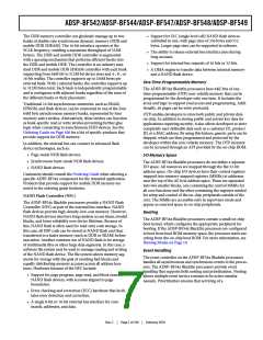
Internal (On-Chip) Memory
0x
2000 0000
RESERVED
The ADSP-BF54x processors have several blocks of on-chip
memory providing high bandwidth access to the core.
The first block is the L1 instruction memory, consisting of
64K bytes of SRAM, of which 16K bytes can be configured as a
four-way set-associative cache or as SRAM. This memory is
accessed at full processor speed.
The second on-chip memory block is the L1 data memory, con-
sisting of 64K bytes of SRAM, of which 32K bytes can be
configured as a two-way set-associative cache or as SRAM. This
memory block is accessed at full processor speed.
TOP OF LAST
DDR PAGE
DDR MEM BANK 1 (8M BYTES to 256M BYTES)
DDR MEM BANK 0 (8M BYTES to 256M BYTES)
0000 0000
0x
Figure 3. ADSP-BF547/ADSP-BF548/ADSP-BF549
Internal/External Memory Map1
1 ForADSP-BF544processors, L2SRAMis64KBytes(0xFEB0000–0xFEB0FFFF).
For ADSP-BF542 processors, there is no L2 SRAM.
External (Off-Chip) Memory
The third memory block is a 4K byte scratchpad SRAM, which
runs at the same speed as the L1 memories. It is only accessible
as data SRAM and cannot be configured as cache memory.
The fourth memory block is the factory programmed L1
instruction ROM, operating at full processor speed. This ROM
is not customer-configurable.
The fifth memory block is the L2 SRAM, providing up to 128K
bytes of unified instruction and data memory, operating at one
half the frequency of the core.
Finally, there is a 4K byte boot ROM connected as L3 memory.
It operates at full SCLK rate.
Through the external bus interface unit (EBIU), the
ADSP-BF54x Blackfin processors provide glueless connectivity
to external 16-bit wide memories, such as DDR and mobile
DDR SDRAM, SRAM, NOR flash, NAND flash, and FIFO
devices. To provide the best performance, the bus system of the
DDR and mobile DDR interface is completely separate from the
other parallel interfaces. Furthermore, the DDR controller sup-
ports either standard DDR memory or mobile DDR memory.
See the Ordering Guide on Page 100 for details. Throughout
this document, references to “DDR” are intended to cover both
the standard and mobile DDR standards.
Rev. C
|
Page 6 of 100
|
February 2010

 ADI [ ADI ]