ADSP-BF542/ADSP-BF544/ADSP-BF547/ADSP-BF548/ADSP-BF549
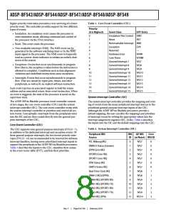
The DDR memory controller can gluelessly manage up to two
• Support for SLC (single level cell) NAND flash devices
unlimited in size, with page sizes of 256 bytes and 512
bytes. Larger page sizes can be supported in software.
• The ability to release external bus interface pins during
long accesses.
• Support for internal bus requests of 16 bits or 32 bits.
• A DMA engine to transfer data between internal memory
and a NAND flash device.
banks of double-rate synchronous dynamic memory (DDR and
mobile DDR SDRAM). The 16-bit interface operates at the
SCLK frequency, enabling a maximum throughput of 532M
bytes/s. The DDR and mobile DDR controller is augmented
with a queuing mechanism that performs efficient bursts into
the DDR and mobile DDR. The controller is an industry stan-
dard DDR and mobile DDR SDRAM controller with each bank
supporting from 64M bit to 512M bit device sizes and 4-, 8-, or
16-bit widths. The controller supports up to 256M bytes per
external bank. With 2 external banks, the controller supports up
to 512M bytes total. Each bank is independently programmable
and is contiguous with adjacent banks regardless of the sizes of
the different banks or their placement.
One-Time-Programmable Memory
The ADSP-BF54x Blackfin processors have 64K bits of one-
time-programmable (OTP) non-volatile memory that can be
programmed by the developer only one time. It includes the
array and logic to support read access and programming. Addi-
tionally, its pages can be write protected.
OTP enables developers to store both public and private data
on-chip. In addition to storing public and private key data for
applications requiring security, it also allows developers to store
completely user-definable data such as a customer ID, product
ID, or a MAC address. By using this feature, generic parts can be
shipped, which are then programmed and protected by the
developer within this non-volatile memory. The OTP memory
can be accessed through an API provided by the on-chip ROM.
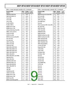
Traditional 16-bit asynchronous memories, such as SRAM,
EPROM, and flash devices, can be connected to one of the four
64M byte asynchronous memory banks, represented by four
memory select strobes. Alternatively, these strobes can function
as bank-specific read or write strobes preventing further glue
logic when connecting to asynchronous FIFO devices. See the
Ordering Guide on Page 100 for a list of specific products that
provide support for DDR memory.
In addition, the external bus can connect to advanced flash
device technologies, such as:
• Page-mode NOR flash devices
• Synchronous burst-mode NOR flash devices
• NAND flash devices
Customers should consult the Ordering Guide when selecting a
specific ADSP-BF54x component for the intended application.
Products that provide support for mobile DDR memory are
noted in the ordering guide footnotes.
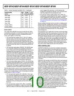
I/O Memory Space
The ADSP-BF54x Blackfin processors do not define a separate
I/O space. All resources are mapped through the flat 32-bit
address space. On-chip I/O devices have their control registers
mapped into memory-mapped registers (MMRs) at addresses
near the top of the 4G byte address space. These are separated
into two smaller blocks, one containing the control MMRs for
all core functions and the other containing the registers needed
for setup and control of the on-chip peripherals outside of the
core. The MMRs are accessible only in supervisor mode and
appear as reserved space to on-chip peripherals.
NAND Flash Controller (NFC)
The ADSP-BF54x Blackfin processors provide a NAND Flash
Controller (NFC) as part of the external bus interface. NAND
flash devices provide high-density, low-cost memory. However,
NAND flash devices also have long random access times, invalid
blocks, and lower reliability over device lifetimes. Because of
this, NAND flash is often used for read-only code storage. In
this case, all DSP code can be stored in NAND flash and then
transferred to a faster memory (such as DDR or SRAM) before
execution. Another common use of NAND flash is for storage
of multimedia files or other large data segments. In this case, a
software file system may be used to manage reading and writing
of the NAND flash device. The file system selects memory seg-
ments for storage with the goal of avoiding bad blocks and
equally distributing memory accesses across all address loca-
tions. Hardware features of the NFC include:
Booting
The ADSP-BF54x Blackfin processors contain a small on-chip
boot kernel, which configures the appropriate peripheral for
booting. If the ADSP-BF54x Blackfin processors are configured
to boot from boot ROM memory space, the processor starts exe-
cuting from the on-chip boot ROM. For more information, see
Booting Modes on Page 19.
Event Handling
The event controller on the ADSP-BF54x Blackfin processors
handles all asynchronous and synchronous events to the proces-
sors. The ADSP-BF54x Blackfin processors provide event
handling that supports both nesting and prioritization. Nesting
allows multiple event service routines to be active simulta-
neously. Prioritization ensures that servicing of a
• Support for page program, page read, and block erase of
NAND flash devices, with accesses aligned to page
boundaries.
• Error checking and correction (ECC) hardware that facili-
tates error detection and correction.
• A single 8-bit or 16-bit external bus interface for com-
mands, addresses, and data.
Rev. C
|
Page 7 of 100
|
February 2010

 ADI [ ADI ]