ADSP-BF542/ADSP-BF544/ADSP-BF547/ADSP-BF548/ADSP-BF549
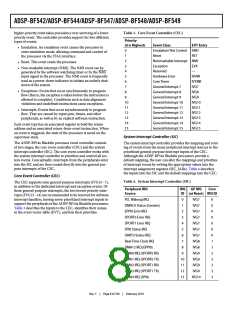
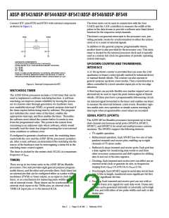
Table 4. System Interrupt Controller (SIC) (Continued)
source triggered the interrupt. A set bit indicates the
peripheral is asserting the interrupt, and a cleared bit indi-
cates the peripheral is not asserting the event.
Peripheral IRQ
Source
IRQ
GP IRQ
Core
ID (at Reset) IRQ ID
• SIC interrupt wakeup enable registers (SIC_IWRx). By
enabling the corresponding bit in this register, a peripheral
can be configured to wake up the processor, should the
core be idled or in Sleep mode when the event is generated.
(For more information, see Dynamic Power Management
on Page 16.)
Because multiple interrupt sources can map to a single general-
purpose interrupt, multiple pulse assertions can occur simulta-
neously, before or during interrupt processing for an interrupt
event already detected on this interrupt input. The IPEND reg-
ister contents are monitored by the SIC as the interrupt
acknowledgement.
Timer 3 IRQ
89
90
91
92
93
94
95
IVG11
IVG11
IVG11
IVG11
IVG11
IVG12
IVG12
4
4
4
4
4
5
5
Timer 4 IRQ
Timer 5 IRQ
Timer 6 IRQ
Timer 7 IRQ
Pin IRQ 2 (PINT2)
Pin IRQ 3 (PINT3)
Event Control
The ADSP-BF54x Blackfin processors provide the user with a
very flexible mechanism to control the processing of events. In
the CEC, three registers are used to coordinate and control
events. Each register is 16 bits wide:
• CEC interrupt latch register (ILAT). The ILAT register
indicates when events have been latched. The appropriate
bit is set when the processor has latched the event and
cleared when the event has been accepted into the system.
This register is updated automatically by the controller, but
it may be written only when its corresponding IMASK bit
is cleared.
The appropriate ILAT register bit is set when an interrupt rising
edge is detected. (Detection requires two core clock cycles.) The
bit is cleared when the respective IPEND register bit is set. The
IPEND bit indicates that the event has entered into the proces-
sor pipeline. At this point the CEC recognizes and queues the
next rising edge event on the corresponding event input. The
minimum latency from the rising edge transition of the general-
purpose interrupt to the IPEND output asserted is three core
clock cycles; however, the latency can be much higher, depend-
ing on the activity within and the state of the processor.
DMA CONTROLLERS
• CEC interrupt mask register (IMASK). The IMASK regis-
ter controls the masking and unmasking of individual
events. When a bit is set in the IMASK register, that event is
unmasked and is processed by the CEC when asserted. A
cleared bit in the IMASK register masks the event, prevent-
ing the processor from servicing the event even though the
event may be latched in the ILAT register. This register
may be read or written while in supervisor mode. Note that
general-purpose interrupts can be globally enabled and dis-
abled with the STI and CLI instructions, respectively.
• CEC interrupt pending register (IPEND). The IPEND reg-
ister keeps track of all nested events. A set bit in the IPEND
register indicates that the event is currently active or nested
at some level. This register is updated automatically by the
controller but may be read while in supervisor mode.
The SIC allows further control of event processing by providing
three 32-bit interrupt control and status registers. Each register
contains a bit corresponding to each of the peripheral interrupt
events shown in Table 4 on Page 8.
• SIC interrupt mask registers (SIC_IMASKx). These regis-
ters control the masking and unmasking of each peripheral
interrupt event. When a bit is set in a register, that periph-
eral event is unmasked and is processed by the system
when asserted. A cleared bit in the register masks the
peripheral event, preventing the processor from servicing
the event.
ADSP-BF54x Blackfin processors have multiple, independent
DMA channels that support automated data transfers with min-
imal overhead for the processor core. DMA transfers can occur
between the ADSP-BF54x processors’ internal memories and
any of the DMA-capable peripherals. Additionally, DMA trans-
fers can be accomplished between any of the DMA-capable
peripherals and external devices connected to the external
memory interfaces, including DDR and asynchronous memory
controllers.
While the USB controller and MXVR have their own dedicated
DMA controllers, the other on-chip peripherals are managed by
two centralized DMA controllers, called DMAC1 (32-bit) and
DMAC0 (16-bit). Both operate in the SCLK domain. Each DMA
controller manages 12 independent peripheral DMA channels,
as well as two independent memory DMA streams. The
DMAC1 controller masters high-bandwidth peripherals over a
dedicated 32-bit DMA access bus (DAB32). Similarly, the
DMAC0 controller masters most serial interfaces over the 16-bit
DAB16 bus. Individual DMA channels have fixed access prior-
ity on the DAB buses. DMA priority of peripherals is managed
by a flexible peripheral-to-DMA channel assignment scheme.
All four DMA controllers use the same 32-bit DCB bus to
exchange data with L1 memory. This includes L1 ROM, but
excludes scratchpad memory. Fine granulation of L1 memory
and special DMA buffers minimize potential memory conflicts
when the L1 memory is accessed simultaneously by the core.
Similarly, there are dedicated DMA buses between the external
bus interface unit (EBIU) and the three DMA controllers
(DMAC1, DMAC0, and USB) that arbitrate DMA accesses to
external memories and the boot ROM.
• SIC interrupt status registers (SIC_ISRx). As multiple
peripherals can be mapped to a single event, these registers
allow the software to determine which peripheral event
Rev. C
|
Page 10 of 100
|
February 2010

 ADI [ ADI ]