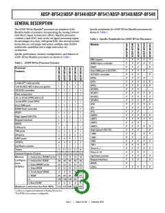
ADSP-BF542/ADSP-BF544/ADSP-BF547/ADSP-BF548/ADSP-BF549
The ADSP-BF54x Blackfin processors are completely code- and
pin-compatible. They differ only with respect to their perfor-
mance, on-chip memory, and selection of I/O peripherals.
Specific performance, memory, and feature configurations are
shown in Table 1.
memory spaces, including external DDR (either standard or
mobile, depending on the device) and asynchronous memory.
Multiple on-chip buses running at up to 133 MHz provide
enough bandwidth to keep the processor core running along
with activity on all of the on-chip and external peripherals.
By integrating a rich set of industry-leading system peripherals
and memory, Blackfin processors are the platform of choice for
next-generation applications that require RISC-like program-
mability, multimedia support, and leading-edge signal
processing in one integrated package.
The ADSP-BF54x Blackfin processors include an on-chip volt-
age regulator in support of the dynamic power management
capability. The voltage regulator provides a range of core volt-
age levels when supplied from VDDEXT. The voltage regulator can
be bypassed at the user’s discretion.
LOW POWER ARCHITECTURE
BLACKFIN PROCESSOR CORE
Blackfin processors provide world-class power management
and performance. Blackfin processors are designed in a low
power and low voltage design methodology and feature on-chip
dynamic power management, the ability to vary both the voltage
and frequency of operation to significantly lower overall power
consumption. Reducing both voltage and frequency can result
in a substantial reduction in power consumption as compared
to reducing only the frequency of operation. This translates into
longer battery life for portable appliances.
As shown in Figure 2 on Page 5, the Blackfin processor core
contains two 16-bit multipliers, two 40-bit accumulators, two
40-bit ALUs, four video ALUs, and a 40-bit shifter. The compu-
tation units process 8-, 16-, or 32-bit data from the register file.
The compute register file contains eight 32-bit registers. When
performing compute operations on 16-bit operand data, the
register file operates as 16 independent 16-bit registers. All
operands for compute operations come from the multiported
register file and instruction constant fields.
SYSTEM INTEGRATION
Each MAC can perform a 16-bit by 16-bit multiply in each
cycle, accumulating the results into the 40-bit accumulators.
Signed and unsigned formats, rounding, and saturation are
supported.
The ADSP-BF54x Blackfin processors are highly integrated
system-on-a-chip solutions for the next generation of embed-
ded network connected applications. By combining industry-
standard interfaces with a high performance signal processing
core, users can develop cost-effective solutions quickly without
the need for costly external components. The system peripherals
include a high speed USB OTG (On-the-Go) controller with
integrated PHY, CAN 2.0B controllers, TWI controllers, UART
ports, SPI ports, serial ports (SPORTs), ATAPI controller,
SD/SDIO controller, a real-time clock, a watchdog timer, LCD
controller, and multiple enhanced parallel peripheral interfaces.
The ALUs perform a traditional set of arithmetic and logical
operations on 16- or 32-bit data. In addition, many special
instructions are included to accelerate various signal processing
tasks. These include bit operations such as field extract and pop-
ulation count, modulo 232 multiply, divide primitives, saturation
and rounding, and sign/exponent detection. The set of video
instructions include byte alignment and packing operations,
16-bit and 8-bit adds with clipping, 8-bit average operations,
and 8-bit subtract/absolute value/accumulate (SAA) operations.
Also provided are the compare/select and vector search
instructions.
For certain instructions, two 16-bit ALU operations can be per-
formed simultaneously on register pairs (a 16-bit high half and
16-bit low half of a compute register). By also using the second
ALU, quad 16-bit operations are possible.
The 40-bit shifter can perform shifts and rotates and is used to
support normalization, field extract, and field deposit
instructions.
The program sequencer controls the flow of instruction execu-
tion, including instruction alignment and decoding. For
program flow control, the sequencer supports PC relative and
indirect conditional jumps (with static branch prediction), and
subroutine calls. Hardware is provided to support zero-over-
head looping. The architecture is fully interlocked, meaning that
the programmer need not manage the pipeline when executing
instructions with data dependencies.
BLACKFIN PROCESSOR PERIPHERALS
The ADSP-BF54x processors contain a rich set of peripherals
connected to the core via several high bandwidth buses, provid-
ing flexibility in system configuration as well as excellent overall
system performance (see Figure 1 on Page 1). The general-
purpose peripherals include functions such as UARTs, SPI,
TWI, timers with pulse width modulation (PWM) and pulse
measurement capability, general-purpose I/O pins, a real-time
clock, and a watchdog timer. This set of functions satisfies a
wide variety of typical system support needs and is augmented
by the system expansion capabilities of the part. The ADSP-
BF54x processors contain dedicated network communication
modules and high speed serial and parallel ports, an interrupt
controller for flexible management of interrupts from the on-
chip peripherals or external sources, and power management
control functions to tailor the performance and power charac-
teristics of the processor and system to many application
scenarios.
The address arithmetic unit provides two addresses for simulta-
neous dual fetches from memory. It contains a multiported
register file consisting of four sets of 32-bit index, modify,
All of the peripherals, except for general-purpose I/O, CAN,
TWI, real-time clock, and timers, are supported by a flexible
DMA structure. There are also separate memory DMA channels
dedicated to data transfers between the processor's various
Rev. C
|
Page 4 of 100
|
February 2010

 ADI [ ADI ]