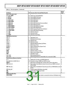
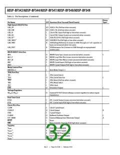
ADSP-BF542/ADSP-BF544/ADSP-BF547/ADSP-BF548/ADSP-BF549
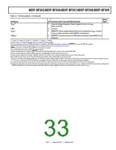
7 Parameter value applies to pins DQ0–15 and DQS0–1.
8 PB1-0, PE15-14, PG15-11, and PH7-6 are 5.0 V-tolerant (always accept up to 5.5 V maximum VIH when power is applied to VDDEXT pins). Voltage compliance (on output
VOH) is limited by VDDEXT supply voltage.
9 SDA and SCL are 5.0V tolerant (always accept up to 5.5V maximum VIH). Voltage compliance on outputs (VOH) is limited by the VDDEXT supply voltage.
10Parameter value applies to USB_DP, USB_DM, and USB_VBUS pins. See Absolute Maximum Ratings on Page 40.
11Parameter value applies to all input and bidirectional pins, except PB1-0, PE15-14, PG15–11, and PH7-6.
12Parameter value applies to pins PG15–11 and PH7-6.
13Parameter value applies to pins PB1-0 and PE15-14. Consult the I2C specification version 2.1 for the proper resistor value and other open drain pin electrical parameters.
14TJ must be in the range: 0°C < TJ < 55°C during OTP memory programming operations.
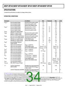
Table 13 and Table 16 describe the voltage/frequency require-
ments for the ADSP-BF54x Blackfin processors’ clocks. Take
care in selecting MSEL, SSEL, and CSEL ratios so as not to
exceed the maximum core clock and system clock. Table 15
describes the phase-locked loop operating conditions.
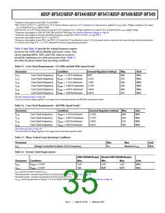
Table 13. Core Clock Requirements—533 MHz and 600 MHz Speed Grade1
Parameter
fCCLK
Condition
Internal Regulator Setting2
Max
600
533
500
444
400
333
Unit
MHz
MHz
MHz
MHz
MHz
MHz
Core Clock Frequency
Core Clock Frequency
Core Clock Frequency
Core Clock Frequency
Core Clock Frequency
Core Clock Frequency
VDDINT = 1.30 V minimum
VDDINT = 1.20 V minimum
VDDINT = 1.14 V minimum
N/A2
fCCLK
1.25 V
1.20 V
fCCLK
fCCLK
VDDINT = 1.045 V minimum 1.10 V
fCCLK
VDDINT = 0.95 V minimum
VDDINT = 0.90 Vminimum
1.00 V
0.95 V
fCCLK
1 See the Ordering Guide on Page 100.
2 Use of an internal voltage regulator is not supported on automotive grade and 600 MHz speed grade models
Table 14. Core Clock Requirements—400 MHz Speed Grade1
Parameter
fCCLK
Condition
Internal Regulator Setting2 Max
Unit
Core Clock Frequency
Core Clock Frequency
Core Clock Frequency
Core Clock Frequency
VDDINT = 1.14 V minimum
VDDINT = 1.045 V minimum
VDDINT = 0.95 V minimum
VDDINT = 0.90 V minimum
1.20 V
1.10 V
1.00 V
0.95 V
400
364
333
300
MHz
MHz
MHz
MHz
fCCLK
fCCLK
fCCLK
1 See Ordering Guide on Page 100
2 Use of an internal voltage regulator is not supported on automotive grade models
Table 15. Phase-Locked Loop Operating Conditions
Parameter
fVCO
Min
50
Max
Maximum fCCLK
Unit
MHz
Voltage Controlled Oscillator (VCO) Frequency
Table 16. System Clock Requirements
DDR SDRAM Models Mobile DDR SDRAM Models
Parameter Condition
Max
1332
100
Min
1203
N/A4
Max
1332
N/A4
Unit
MHz
MHz
fSCLK
VDDINT ≥ 1.14 V1
fSCLK
VDDINT < 1.14 V1
1 fSCLK must be less than or equal to fCCLK
.
2 Rounded number. Actual test specification is SCLK period of 7.5 ns. See Table 26 on Page 43.
3 Rounded number. Actual test specification is SCLK period of 8.33 ns.
4 VDDINT must be greater than or equal to 1.14 V for mobile DDR SDRAM models. See Operating Conditions on Page 34.
Rev. C
|
Page 35 of 100
|
February 2010

 ADI [ ADI ]