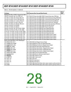
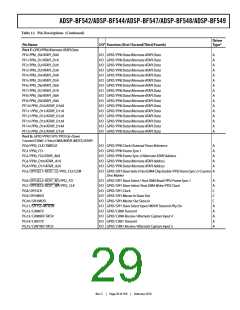
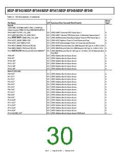
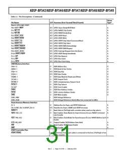
ADSP-BF542/ADSP-BF544/ADSP-BF547/ADSP-BF548/ADSP-BF549
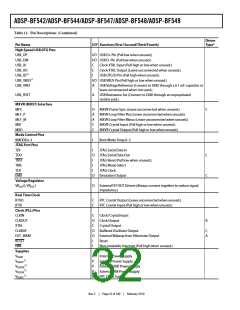
Table 12. Pin Descriptions (Continued)
Driver
Type2
Pin Name
I/O1 Function (First/Second/Third/Fourth)
High Speed USB OTG Pins
USB_DP
USB_DM
I/O USB D+ Pin (Pull low when unused.)
I/O USB D- Pin (Pull low when unused.)
USB_XI
USB_XO
USB_ID10
C
C
I
Clock XTAL Input (Pull high or low when unused.)
Clock XTAL Output (Leave unconnected when unused.)
USB OTG ID Pin (Pull high when unused.)
USB_VBUS11
USB_VREF
I/O USB VBUS Pin (Pull high or low when unused.)
A
USB Voltage Reference (Connect to GND through a 0.1 mF capacitor or
leave unconnected when not used.)
USB_RSET
A
USB Resistance Set (Connect to GND through an unpopulated
resistor pad.)
MXVR (MOST) Interface
MFS
MLF_P
MLF_M
MXI
O
A
A
C
C
MXVR Frame Sync (Leave unconnected when unused.)
MXVR Loop Filter Plus (Leave unconnected when unused.)
MXVR Loop Filter Minus (Leave unconnected when unused.)
MXVR Crystal Input (Pull high or low when unused.)
MXVR Crystal Output (Pull high or low when unused.)
C
MXO
Mode Control Pins
BMODE0–3
I
Boot Mode Strap 0–3
JTAG Port Pins
TDI
TDO
TRST
TMS
I
O
I
JTAG Serial Data In
JTAG Serial Data Out
JTAG Reset (Pull low when unused.)
JTAG Mode Select
C
C
I
TCK
EMU
I
O
JTAG Clock
Emulation Output
Voltage Regulator
VROUT0, VROUT
1
O
External FET/BJT Drivers (Always connect together to reduce signal
impedance.)
Real Time Clock
RTXO
RTXI
C
C
RTC Crystal Output (Leave unconnected when unused.)
RTC Crystal Input (Pull high or low when unused.)
Clock (PLL) Pins
CLKIN
CLKOUT
XTAL
CLKBUF
EXT_WAKE
RESET
C
O
C
O
O
I
Clock/Crystal Input
Clock Output
Crystal Output
Buffered Oscillator Output
External Wakeup from Hibernate Output
Reset
B
C
A
NMI
I
Non-maskable Interrupt (Pull high when unused.)
Supplies
VDDINT
P
P
P
P
P
Internal Power Supply
External Power Supply
External DDR Power Supply
External USB Power Supply
RTC Clock Supply
12
VDDEXT
VDDDDR
VDDUSB
12
12
12
VDDRTC
Rev. C
|
Page 32 of 100
|
February 2010

 ADI [ ADI ]