ADSP-BF542/ADSP-BF544/ADSP-BF547/ADSP-BF548/ADSP-BF549
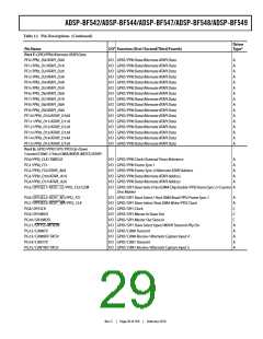
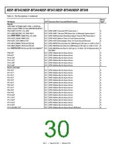
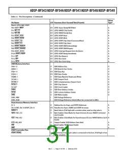
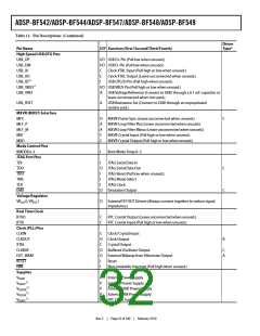
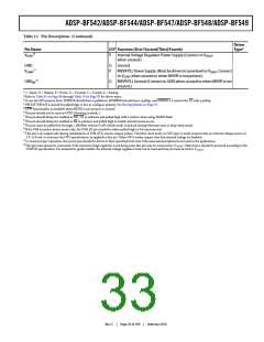
Table 12. Pin Descriptions (Continued)
Driver
Type2
Pin Name
VDDVR
I/O1 Function (First/Second/Third/Fourth)
13
P
Internal Voltage Regulator Power Supply (Connect to VDDEXT
when unused.)
GND
VDDMP
G
P
Ground
12
MXVR PLL Power Supply. (Must be driven to same level as VDDINT. Connect
to VDDINT when unused or when MXVR is not present.)
MXVR PLL Ground (Connect to GND when unused or when MXVR is not
present.)
12
GNDMP
G
1 I = Input, O = Output, P =Power, G = Ground, C = Crystal, A = Analog.
2 Refer to Table 61 on Page 86 through Table 70 on Page 87 for driver types.
3 To use the SPI memory boot, SPI0SCK should have a pulldown, SPI0MISO should have a pullup, and SPI0SEL1 is used as the CS with a pullup.
4 HWAIT/HWAITA should be pulled high or low to configure polarity. See Booting Modes on Page 19.
5 GPW functionality is available when MXVR is not present or unused.
6 This pin should not be used as GPIO if booting in mode 1.
7 This pin should always be enabled as ND_CE in software and pulled high with a resistor when using NAND flash.
8 This pin should always be enabled as BR in software and pulled high to enable asynchronous access.
9 This pin must be pulled low through a 10kOhm resistor if self-refresh mode is desired during hibernate state or deep-sleep mode.
10If the USB is used in device mode only, the USB_ID pin should be either pulled high or left unconnected.
11This pin is an output only during initialization of USB OTG session request pulses. Therefore, host mode or OTG type A mode requires that an external voltage source of
5 V, at 8 mA or more per the OTG specification, be applied to this pin. Other OTG modes require that this external voltage be disabled.
12To ensure proper operation, the power pins should be driven to their specified level even if the associated peripheral is not used in the application.
13This pin must always be connected. If the internal voltage regulator is not being used, this pin may be connected to VDDEXT. Otherwise it should be powered according to the
VDDVR specification. For automotive grade models, the internal voltage regulator must not be used and this pin must be tied to VDDEXT
.
Rev. C
|
Page 33 of 100
|
February 2010

 ADI [ ADI ]