ADSP-BF542/ADSP-BF544/ADSP-BF547/ADSP-BF548/ADSP-BF549
13See the ADSP-BF54x Blackfin Processor Hardware Reference Manual for definition of sleep, deep sleep, and hibernate operating modes.
14Includes current on VDDEXT, VDDUSB, VDDVR, and VDDDDR supplies. Clock inputs are tied high or low.
15Guaranteed maximum specifications.
16Unit for VDDINT is V (volts). Unit for fSCLK is MHz. Example: 1.2 V, 133 MHz would be 0.77 × 1.2 × 133 = 122.9 mA added to IDDDEEPSLEEP
.
17See Table 19 for the list of IDDINT power vectors covered.
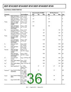
Total power dissipation has two components:
• Static, including leakage current
• Dynamic, due to transistor switching characteristics
Many operating conditions can also affect power dissipation,
including temperature, voltage, operating frequency, and pro-
cessor activity. Electrical Characteristics on Page 36 shows the
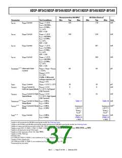
current dissipation for internal circuitry (VDDINT). IDDDEEPSLEEP
specifies static power dissipation as a function of voltage
(VDDINT) and temperature (see Table 17 and Table 18), and
IDDINT specifies the total power specification for the listed test
conditions, including the dynamic component as a function of
voltage (VDDINT) and frequency (Table 20).
There are two parts to the dynamic component. The first part is
due to transistor switching in the core clock (CCLK) domain.
This part is subject to an activity scaling factor (ASF) which rep-
resents application code running on the processor core and
L1/L2 memories (Table 19). The ASF is combined with the
CCLK frequency and VDDINT dependent data in Table 20 to cal-
culate this part. The second part is due to transistor switching in
the system clock (SCLK) domain, which is included in the IDDINT
specification equation.
Table 17. Static Current—Nonautomotive 400 MHz Speed Grade Devices (mA)1
2
Voltage (VDDINT
)
TJ (°C)2 0.90 V 0.95 V 1.00 V 1.05 V 1.10 V 1.15 V 1.20 V 1.25 V 1.30 V 1.35 V 1.38 V 1.40 V 1.43 V
-40
0
11.9
20.1
31.2
47.0
58.6
80.7
107.0
153.9
171.7
13.5
22.3
34.2
51.0
63.1
86.6
114.3
163.0
181.5
15.5
24.7
37.5
55.5
68.3
93.0
122.5
173.3
192.7
17.7
20.3
23.3
26.8
30.6
35.0
39.9
43.2
45.5
49.5
27.8
31.1
34.9
39.3
44.2
49.6
55.7
59.8
62.5
67.2
25
45
55
70
85
100
105
41.3
45.6
50.3
55.7
61.7
68.2
75.4
80.3
83.6
88.6
60.6
66.0
72.0
78.8
86.1
94.2
102.9
122.0
158.7
202.7
272.4
299.3
108.9
128.4
166.4
211.8
283.4
308.7
112.8
132.8
171.6
218.0
290.8
314.9
118.2
140.0
179.5
226.7
300.6
325.7
74.1
80.3
87.1
94.9
103.0
136.0
175.3
239.0
263.6
112.0
146.8
188.5
255.1
280.9
100.2
131.5
184.8
205.1
108.1
141.2
197.0
218.3
116.7
151.7
210.0
232.4
125.9
163.1
224.1
247.5
1 Values are guaranteed maximum IDDDEEPSLEEP for nonautomotive 400 MHz speed-grade devices.
2 Valid temperature and voltage ranges are model-specific. See Operating Conditions on Page 34.
Table 18. Static Current—Automotive 400 MHz and All 533 MHz/600 MHz Speed Grade Devices (mA)1
2
Voltage (VDDINT
)
TJ (°C)2
-40
0
0.90 V 0.95 V 1.00 V 1.05 V 1.10 V 1.15 V 1.20 V 1.25 V 1.30 V 1.35 V 1.38 V 1.40 V 1.43 V
19.7
22.1
24.8
27.9
31.4
35.4
39.9
45.0
50.6
57.0
61.2
64.0
70.4
45.2
49.9
55.2
61.3
67.9
75.3
83.5
92.6
102.6
169.2
247.6
299.7
394.3
516.5
654.8
711.1
113.6
185.4
269.6
325.9
427.7
557.5
704.7
763.9
121.0
196.1
284.0
343.1
449.4
584.2
737.0
798.5
125.8
203.3
293.6
354.6
463.9
602.0
758.5
821.6
135.0
218.0
312.0
374.0
489.0
629.0
793.0
864.0
25
80.0
87.5
96.2
105.8
160.7
197.7
264.1
350.2
452.1
494.3
116.4
175.3
214.9
285.8
378.5
486.9
531.7
127.9
191.2
233.8
309.4
408.9
524.4
571.9
140.4
208.6
254.2
334.8
442.1
564.8
614.9
154.1
227.3
276.1
363.5
477.9
608.2
661.5
45
124.2
154.6
209.8
281.8
366.5
403.8
134.8
167.2
225.6
301.3
390.5
428.3
147.1
181.7
243.9
323.5
419.4
459.5
55
70
85
100
105
1 Values are guaranteed maximum IDDDEEPSLEEP for automotive 400 MHz and all 533 MHz and 600 MHz speed grade devices.
2 Valid temperature and voltage ranges are model-specific. See Operating Conditions on Page 34.
Rev. C
|
Page 38 of 100
|
February 2010

 ADI [ ADI ]