ADSP-BF542/ADSP-BF544/ADSP-BF547/ADSP-BF548/ADSP-BF549
SPECIFICATIONS
Component specifications are subject to change without notice.
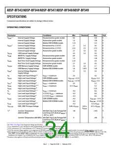
OPERATING CONDITIONS
Parameter
VDDINT
Conditions
Min
0.9
Nominal
Max
1.43
1.38
1.31
3.6
Unit
V
1, 2
Internal Supply Voltage
Internal Supply Voltage
Internal Supply Voltage
External Supply Voltage
External Supply Voltage
External Supply Voltage
USB External Supply Voltage
MXVR PLL Supply Voltage
MXVR PLL Supply Voltage
Nonautomotive grade models
Automotive grade models
Mobile DDR SDRAM models
Nonautomotive 3.3 V I/O
Nonautomotive 2.5 V I/O
Automotive grade models
1.0
V
1.14
2.7
V
3
VDDEXT
3.3
2.5
3.3
3.3
V
2.25
2.7
2.75
3.6
V
V
VDDUSB
VDDMP
3.0
3.6
V
Nonautomotive grade models
Automotive grade models
0.9
1.43
1.38
3.6
V
1.0
V
VDDRTC
VDDDDR
Real Time Clock Supply Voltage Nonautomotive grade models
Real Time Clock Supply Voltage Automotive grade models
2.25
2.7
V
3.3
2.6
3.6
V
DDR Memory Supply Voltage
DDR Memory Supply Voltage
DDR SDRAM models
2.5
2.7
V
Mobile DDR SDRAM models
1.8
1.875
3.3
1.95
3.6
V
4
VDDVR
Internal Voltage Regulator
Supply Voltage
2.7
V
VIH
High Level Input Voltage5, 6
High Level Input Voltage7
High Level Input Voltage7
High Level Input Voltage8
High Level Input Voltage 9, 13
High Level Input Voltage10
Low Level Input Voltage5, 11
Low Level Input Voltage12
Low Level Input Voltage12
Low Level Input Voltage7
Low Level Input Voltage7
Low Level Input Voltage9, 13
DDR_VREF Pin Input Voltage
VDDEXT = maximum
2.0
3.6
V
V
V
V
V
V
V
V
V
V
VIHDDR
DDR SDRAM models
Mobile DDR SDRAM models
VDDEXT = maximum
VDDR_VREF + 0.15
VDDR_VREF + 0.125
2.0
VDDDDR + 0.3
VDDDDR + 0.3
12
VIH5V
5.5
VIHTWI
VIHUSB
VIL
VDDEXT = maximum
0.7 x VDDEXT
5.5
5.25
VDDEXT = minimum
–0.3
–0.3
0.6
VIL5V
3.3 V I/O, VDDEXT = minimum
2.5 V I/O, VDDEXT = minimum
DDR SDRAM models
0.8
0.6
–0.3
VILDDR
–0.3
VDDR_VREF – 0.15
Mobile DDR SDRAM models
–0.3
VDDR_VREF – 0.125 V
VILTWI
–0.3
0.3 x VDDEXT
V
V
VDDR_VREF
0.49 x VDDDDR
0.50 x
VDDDDR
0.51 x VDDDDR
TJ14
Junction Temperature
(400/533 MHz)
400-Ball Chip Scale Package Ball
–40
0
+105
+90
ºC
Grid Array (CSP_BGA) @TAMBIENT
=
–40ºC to +85ºC
Junction Temperature (600 MHz) 400-Ball Chip Scale Package Ball
ºC
Grid Array (CSP_BGA) @TAMBIENT
=
0ºC to +70ºC
1 See Table 13 on Page 35 for frequency/voltage specifications.
2 VDDINT maximum is 1.10 V during one-time-programmable (OTP) memory programming operations.
3 VDDEXT minimum is 3.0 V and maximum is 3.6 V during OTP memory programming operations.
4 Use of the internal voltage regulator is not supported on 600 MHz speed grade models or on automotive grade models. An external voltage regulator must be used.
5 Bidirectional pins (D15–0, PA15–0, PB14–0, PC15–0, PD15–0, PE15–0, PF15–0, PG15–0, PH13–0, PI15–0, PJ14–0) and input pins (ATAPI_PDIAG, USB_ID, TCK, TDI,
TMS, TRST, CLKIN, RESET, NMI, and BMODE3–0) of the ADSP-BF54x Blackfin processors are 3.3 V-tolerant (always accept up to 3.6 V maximum VIH). Voltage
compliance (on outputs, VOH) is limited by the VDDEXT supply voltage. The regulator can generate VDDINT at levels of 0.90 V to 1.30 V with -5% to +5% tolerance.
6 Parameter value applies to all input and bidirectional pins except PB1-0, PE15-14, PG15–11, PH7-6, DQ0-15, and DQS0-1.
Rev. C
|
Page 34 of 100
|
February 2010

 ADI [ ADI ]