ADSP-BF542/ADSP-BF544/ADSP-BF547/ADSP-BF548/ADSP-BF549
key is meant to be pressed. It is possible to detect when multiple
keys are pressed simultaneously and to provide limited key reso-
lution capability when this happens.
Interrupts are generated when a user-defined amount of syn-
chronous data has been sent or received by the processor or
when asynchronous packets or control messages have been sent
or received.
SECURE DIGITAL (SD)/SDIO CONTROLLER
The SD/SDIO controller is a serial interface that stores data at a
data rate of up to 10M bytes per second using a 4-bit data line.
The SD/SDIO controller supports the SD memory mode only.
The interface supports all the power modes and performs error
checking by CRC.
The MXVR peripheral can wake up the ADSP-BF549 Blackfin
processor from sleep mode when a wakeup preamble is received
over the network or based on any other MXVR interrupt event.
Additionally, detection of network activity by the MXVR can be
used to wake up the ADSP-BF549 Blackfin processor from the
hibernate state. These features allow the ADSP-BF549 processor
to operate in a low-power state when there is no network activ-
ity or when data is not currently being received or transmitted
by the MXVR.
The MXVR clock is provided through a dedicated external crys-
tal or crystal oscillator. The frequency of the external crystal or
crystal oscillator can be 256 Fs, 384 Fs, 512 Fs, or 1024 Fs for
Fs = 38 kHz, 44.1 kHz, or 48 kHz. If using a crystal to provide
the MXVR clock, use a parallel-resonant, fundamental mode,
microprocessor-grade crystal.
CODE SECURITY
An OTP/security system, consisting of a blend of hardware and
software, provides customers with a flexible and rich set of code
security features with Lockbox® secure technology. Key features
include:
• OTP memory
• Unique chip ID
• Code authentication
• Secure mode of operation
The security scheme is based upon the concept of authentica-
tion of digital signatures using standards-based algorithms and
provides a secure processing environment in which to execute
code and protect assets. See Lockbox Secure Technology Dis-
claimer on Page 24.
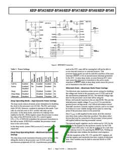
DYNAMIC POWER MANAGEMENT
The ADSP-BF54x Blackfin processors provide five operating
modes, each with a different performance/power profile. In
addition, dynamic power management provides the control
functions to dynamically alter the processor core supply voltage,
further reducing power dissipation. Control of clocking to each
of the ADSP-BF54x Blackfin processors’ peripherals also
reduces power consumption. See Table 5 for a summary of the
power settings for each mode.
MEDIA TRANSCEIVER MAC LAYER (MXVR)
The ADSP-BF549 Blackfin processors provide a media trans-
ceiver (MXVR) MAC layer, allowing the processor to be
connected directly to a MOST® 1 network through an FOT. See
Figure 5 on Page 17 for an example of a MXVR MOST
connection.
The MXVR is fully compatible with industry-standard standal-
one MOST controller devices, supporting 22.579 Mbps or
24.576 Mbps data transfer. It offers faster lock times, greater jit-
ter immunity, and a sophisticated DMA scheme for data
transfers. The high speed internal interface to the core and L1
memory allows the full bandwidth of the network to be utilized.
The MXVR can operate as either the network master or as a net-
work slave.
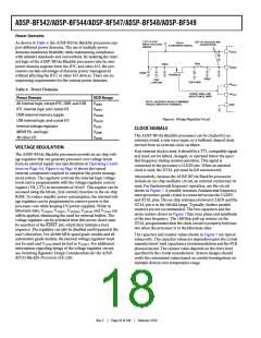
Full-On Operating Mode—Maximum Performance
In the full-on mode, the PLL is enabled and is not bypassed,
providing the capability to run at the maximum operational fre-
quency. This is the power-up default execution state in which
maximum performance can be achieved. The processor core
and all enabled peripherals run at full speed.
Active Operating Mode—Moderate Power Savings
In the active mode, the PLL is enabled but bypassed. Because the
PLL is bypassed, the processor’s core clock (CCLK) and system
clock (SCLK) run at the input clock (CLKIN) frequency. DMA
access is available to appropriately configured L1 memories.
The MXVR supports synchronous data, asynchronous packets,
and control messages using dedicated DMA channels that oper-
ate autonomously from the processor core moving data to and
from L1 and/or L2 memory. Synchronous data is transferred to
or from the synchronous data physical channels on the MOST
bus through eight programmable DMA channels. The synchro-
nous data DMA channels can operate in various modes
including modes that trigger DMA operation when data pat-
terns are detected in the receive data stream. Furthermore, two
DMA channels support asynchronous traffic, and two others
support control message traffic.
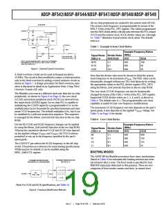
In the active mode, it is possible to disable the control input to
the PLL by setting the PLL_OFF bit in the PLL control register.
This register can be accessed with a user-callable routine in the
on-chip ROM called bfrom_SysControl(). For more informa-
tion, see the “Dynamic Power Management” chapter in the
ADSP-BF54x Blackfin Processor Hardware Reference. If dis-
abled, the PLL must be re-enabled before transitioning to the
full-on or sleep modes.
1 MOST is a registered trademark of Standard Microsystems, Corp.
Rev. C
|
Page 16 of 100
|
February 2010

 ADI [ ADI ]