ADSP-BF542/ADSP-BF544/ADSP-BF547/ADSP-BF548/ADSP-BF549
modes, the processor actively loads data from parallel or serial
memories. In slave boot modes, the processor receives data
from an external host device.
performs an 8- or 16-bit boot or starts program execution
at the address provided by the header. By default, all con-
figuration settings are set for the slowest device possible (3-
cycle hold time; 15-cycle R/W access times; 4-cycle setup).
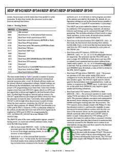
Table 9. Booting Modes
The ARDY pin is not enabled by default. It can, however,
be enabled by OTP programming. Similarly, all interface
behavior and timings can be customized through OTP pro-
gramming. This includes activation of burst-mode or page-
mode operation. In this mode, all asynchronous interface
signals are enabled at the port muxing level.
• Boot from 16-bit asynchronous FIFO (BMODE = 0x2)—In
this mode, the boot kernel starts booting from address
0x2030 0000. Every 16-bit word that the boot kernel has to
read from the FIFO must be requested by a low pulse on
the DMAR1 pin.
• Boot from serial SPI memory, EEPROM or flash
(BMODE = 0x3)—8-, 16-, 24- or 32-bit addressable devices
are supported. The processor uses the PE4 GPIO pin to
select a single SPI EEPROM or flash device and uses SPI0
to submit a read command and successive address bytes
(0x00) until a valid 8-, 16-, 24-, or 32-bit addressable device
is detected. Pull-up resistors are required on the SPI0SEL1
and SPI0MISO pins. By default, a value of 0x85 is written to
the SPI0_BAUD register.
• Boot from SPI host device (BMODE = 0x4)—The proces-
sor operates in SPI slave mode (using SPI0) and is
configured to receive the bytes of the .LDR file from an SPI
host (master) agent. The HWAIT signal must be interro-
gated by the host before every transmitted byte. A pull-up
resistor is required on the SPI0SS input. A pull-down resis-
tor on the serial clock (SPI0SCK) may improve signal
quality and booting robustness.
• Boot from serial TWI memory, EEPROM or flash
(BMODE = 0x5)—The processor operates in master mode
(using TWI0) and selects the TWI slave with the unique ID
0xA0. The processor submits successive read commands to
the memory device starting at two-byte internal address
0x0000 and begins clocking data into the processor. The
TWI memory device should comply with Philips I2C Bus
Specification version 2.1 and have the capability to auto-
increment its internal address counter such that the con-
tents of the memory device can be read sequentially. By
default, a prescale value of 0xA and CLKDIV value of
0x0811 is used. Unless altered by OTP settings, an I2C
memory that takes two address bytes is assumed. Develop-
ment tools ensure that data that is booted to memories that
cannot be accessed by the Blackfin core is written to an
intermediate storage place and then copied to the final des-
tination via memory DMA.
BMODE3–0 Description
0000
0001
0010
0011
0100
0101
0110
0111
1000
1001
1010
1011
1100
1101
1110
1111
Idle-no boot
Boot from 8- or 16-bit external flash memory
Boot from 16-bit asynchronous FIFO
Boot from serial SPI memory (EEPROM or flash)
Boot from SPI host device
Boot from serial TWI memory (EEPROM or flash)
Boot from TWI host
Boot from UART host
Reserved
Reserved
Boot from DDR SDRAM/Mobile DDR SDRAM
Boot from OTP memory
Reserved
Boot from 8- or16-bit NANDflash memory via NFC
Boot from 16-bit host DMA
Boot from 8-bit host DMA
The boot modes listed in Table 9 provide a number of mecha-
nisms for automatically loading the processor’s internal and
external memories after a reset. By default, all boot modes use
the slowest allowed configuration settings. Default settings can
be altered via the initialization code feature at boot time or by
proper OTP programming at pre-boot time. Some boot modes
require a boot host wait (HWAIT) signal, which is a GPIO out-
put signal that is driven and toggled by the boot kernel at boot
time. If pulled high through an external pull-up resistor, the
HWAIT signal behaves active high and will be driven low when
the processor is ready for data. Conversely, when pulled low,
HWAIT is driven high when the processor is ready for data.
When the boot sequence completes, the HWAIT pin can be
used for other purposes. By default, HWAIT functionality is on
GPIO port B (PB11). However, if PB11 is otherwise utilized in
the system, an alternate boot host wait (HWAITA) signal can be
enabled on GPIO port H (PH7) by programming the
OTP_ALTERNATE_HWAIT bit in the PBS00L OTP
memory page.
The BMODE pins of the reset configuration register, sampled
during power-on resets and software-initiated resets, imple-
ment the following modes:
• Idle-no boot mode (BMODE = 0x0)—In this mode, the
processor goes into the idle state. The idle boot mode helps
to recover from illegal operating modes, in case the OTP
memory is misconfigured.
• Boot from TWI host (BMODE = 0x6)—The TWI host
agent selects the slave with the unique ID 0x5F. The proces-
sor (using TWI0) replies with an acknowledgement, and
the host can then download the boot stream. The TWI host
agent should comply with Philips I2C Bus Specification ver-
• Boot from 8- or 16-bit external flash memory—
(BMODE = 0x1)—In this mode, the boot kernel loads the
first block header from address 0x2000 0000 and, depend-
ing on instructions contained in the header, the boot kernel
Rev. C
|
Page 20 of 100
|
February 2010

 ADI [ ADI ]