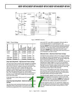
ADSP-BF542/ADSP-BF544/ADSP-BF547/ADSP-BF548/ADSP-BF549
The following features are supported in the EPPI module:
• Programmable data length: 8 bits, 10 bits, 12 bits, 14 bits,
16 bits, 18 bits, and 24 bits per clock.
• Bidirectional and half-duplex port.
• Clock can be provided externally or can be generated
internally.
• Various framed and non-framed operating modes. Frame
syncs can be generated internally or can be supplied by an
external device.
• Various general-purpose modes with zero to three frame
syncs for both receive and transmit directions.
• ITU-656 status word error detection and correction for
ITU-656 receive modes.
• ITU-656 preamble and status word decode.
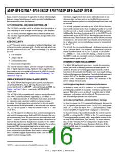
The USB clock (USB_XI) is provided through a dedicated exter-
nal crystal or crystal oscillator. See Table 62 for related timing
requirements. If using a fundamental mode crystal to provide
the USB clock, connect the crystal between USB_XI and
USB_XO with a circuit similar to that shown in Figure 7. Use a
parallel-resonant, fundamental mode, microprocessor-grade
crystal. If a third-overtone crystal is used, follow the circuit
guidelines outlined in Clock Signals on Page 18 for third-over-
tone crystals.
The USB On-the-Go dual-role device controller includes a
Phase Locked Loop with programmable multipliers to generate
the necessary internal clocking frequency for USB. The multi-
plier value should be programmed based on the USB_XI clock
frequency to achieve the necessary 480 MHz internal clock for
USB high speed operation. For example, for a USB_XI crystal
frequency of 24 MHz, the USB_PLLOSC_CTRL register should
be programmed with a multiplier value of 20 to generate a 480
MHz internal clock.
• Three different modes for ITU-656 receive modes: active
video only, vertical blanking only, and entire field mode.
ATA/ATAPI-6 INTERFACE
• Horizontal and vertical windowing for GP 2 and 3 frame
sync modes.
• Optional packing and unpacking of data to/from 32 bits
from/to 8, 16 and 24 bits. If packing/unpacking is enabled,
endianness can be changed to change the order of pack-
ing/unpacking of bytes/words.
• Optional sign extension or zero fill for receive modes.
• During receive modes, alternate even or odd data samples
can be filtered out.
• Programmable clipping of data values for 8-bit transmit
modes.
• RGB888 can be converted to RGB666 or RGB565 for trans-
mit modes.
The ATAPI interface connects to CD/DVD and HDD drives
and is ATAPI-6 compliant. The controller implements the
peripheral I/O mode, the multi-DMA mode, and the Ultra
DMA mode. The DMA modes enable faster data transfer and
reduced host management. The ATAPI controller supports
PIO, multi-DMA, and ultra DMA ATAPI accesses. Key features
include:
• Supports PIO modes 0, 1, 2, 3, 4
• Supports multiword DMA modes 0, 1, 2
• Supports ultra DMA modes 0, 1, 2, 3, 4, 5 (up to UDMA
100)
• Programmable timing for ATA interface unit
• Supports CompactFlash cards using true IDE mode
• Various de-interleaving/interleaving modes for receiv-
ing/transmitting 4:2:2 YCrCb data.
• FIFO watermarks and urgent DMA features.
• Clock gating by an external device asserting the clock gat-
ing control signal.
• Configurable LCD data enable (DEN) output available on
Frame Sync 3.
By default, the ATAPI_A0-2 address signals and the
ATAPI_D0-15 data signals are shared on the asynchronous
memory interface with the asynchronous memory and NAND
flash controllers. The data and address signals can be remapped
to GPIO ports F and G, respectively, by setting
PORTF_MUX[1:0] to b#01.
KEYPAD INTERFACE
USB ON-THE-GO DUAL-ROLE DEVICE
CONTROLLER
The keypad interface is a 16-pin interface module that is used to
detect the key pressed in a 8 × 8 (maximum) keypad matrix. The
size of the input keypad matrix is programmable. The interface
is capable of filtering the bounce on the input pins, which is
common in keypad applications. The width of the filtered
bounce is programmable. The module is capable of generating
an interrupt request to the core once it identifies that any key
has been pressed.
The interface supports a press-release-press mode and infra-
structure for a press-hold mode. The former mode identifies a
press, release and press of a key as two consecutive presses of the
same key, whereas the latter mode checks the input key’s state in
periodic intervals to determine the number of times the same
The USB OTG dual-role device controller (USBDRC) provides
a low-cost connectivity solution for consumer mobile devices
such as cell phones, digital still cameras, and MP3 players,
allowing these devices to transfer data using a point-to-point
USB connection without the need for a PC host. The USBDRC
module can operate in a traditional USB peripheral-only mode
as well as the host mode presented in the On-the-Go (OTG)
supplement to the USB 2.0 specification. In host mode, the USB
module supports transfers at high speed (480 Mbps), full speed
(12 Mbps), and low speed (1.5 Mbps) rates. Peripheral-only
mode supports the high and full speed transfer rates.
Rev. C
|
Page 15 of 100
|
February 2010

 ADI [ ADI ]