ADSP-BF542/ADSP-BF544/ADSP-BF547/ADSP-BF548/ADSP-BF549
All on-chip peripherals are clocked by the system clock (SCLK).
BLACKFIN
The system clock frequency is programmable by means of the
SSEL3–0 bits of the PLL_DIV register. The values programmed
into the SSEL fields define a divide ratio between the PLL output
(VCO) and the system clock. SCLK divider values are 1 through
15. Table 7 illustrates typical system clock ratios. The default
ratio is 4.
CLKOUT
CLKBUF
TO PLL CIRCUITRY
EN
700ꢀ
EN
V
DDEXT
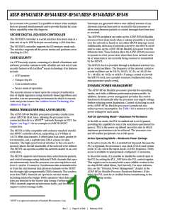
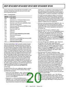
Table 7. Example System Clock Ratios
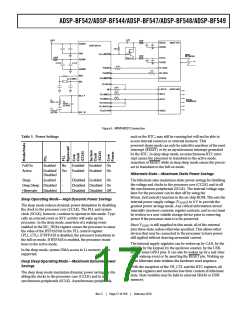
XTAL
CLKIN
*
0 ꢀ
1Mꢀ
Example Frequency Ratios
(MHz)
VCO
200
Signal Name Divider Ratio
18 pF*
18 pF*
FOR OVERTONE
OPERATION ONLY
SSEL3–0
VCO/SCLK
SCLK
100
50
NOTE: VALUES MARKED WITH * MUST BE CUSTOMIZED
DEPENDING ON THE CRYSTAL AND LAYOUT. PLEASE
ANALYZE CAREFULLY.
0010
2:1
0110
6:1
300
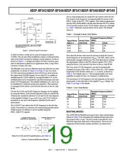
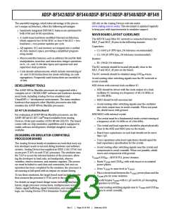
Figure 7. External Crystal Connections
1010
10:1
500
50
A third-overtone crystal can be used at frequencies above
25 MHz. The circuit is then modified to ensure crystal operation
only at the third overtone by adding a tuned inductor circuit as
shown in Figure 7. A design procedure for third-overtone oper-
ation is discussed in detail in an Application Note, Using Third
Overtone Crystals (EE-168).
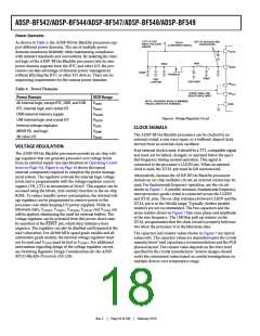
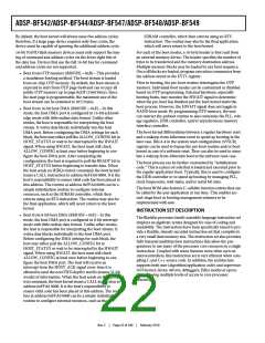
The Blackfin core runs at a different clock rate than the on-chip
peripherals. As shown in Figure 8 on Page 19, the core clock
(CCLK) and system peripheral clock (SCLK) are derived from
the input clock (CLKIN) signal. An on-chip PLL is capable of
multiplying the CLKIN signal by a programmable 0.5× to 64×
multiplication factor (bounded by specified minimum and max-
imum VCO frequencies). The default multiplier is 8×, but it can
be modified by a software instruction sequence. This sequence
is managed by the bfrom_SysControl() function in the on-chip
ROM.
Note that the divisor ratio must be chosen to limit the system
clock frequency to its maximum of fSCLK. The SSEL value can be
dynamically changed without any PLL lock latencies by writing
the appropriate values to the PLL divisor register (PLL_DIV)
using the bfrom_SysControl() function in the on-chip ROM.
The core clock (CCLK) frequency can also be dynamically
changed by means of the CSEL1–0 bits of the PLL_DIV register.
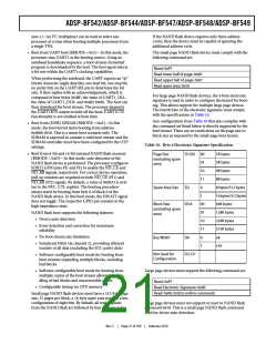
Supported CCLK divider ratios are 1, 2, 4, and 8, as shown in
Table 8. The default ratio is 1. This programmable core clock
capability is useful for fast core frequency modifications.
The maximum CCLK frequency not only depends on the part’s
speed grade, it also depends on the applied VDDINT voltage. See
Table 13 on Page 35 for details.
Table 8. Core Clock Ratios
On-the-fly CCLK and SCLK frequency changes can be applied
by using the bfrom_SysControl() function in the on-chip ROM.
Whereas the maximum allowed CCLK and SCLK rates depend
on the applied voltages VDDINT and VDDEXT, the VCO is always
permitted to run up to the frequency specified by the part’s
speed grade.
The CLKOUT pin reflects the SCLK frequency to the off-chip
world. It functions as a reference for many timing specifications.
While inactive by default, it can be enabled using the
EBIU_AMGCTL register.
Example Frequency Ratios
(MHz)
VCO
300
Signal Name Divider Ratio
CSEL1–0
VCO/CCLK
CCLK
300
150
125
25
00
01
10
11
1:1
2:1
4:1
8:1
300
500
200
BOOTING MODES
The ADSP-BF54x Blackfin processors have many mechanisms
(listed in Table 9) for automatically loading internal and exter-
nal memory after a reset. The boot mode is specified by four
BMODE input pins dedicated to this purpose. There are two
categories of boot modes: master and slave. In master boot
DYNAMIC MODIFICATION
ON-THE-FLY
DYNAMIC MODIFICATION
REQUIRES PLL SEQUENCING
CCLK
SCLK
1, 2, 4, 8
ꢁ
PLL
0.5x - 64x
CLKIN
VCO
ꢁ 1:15
Note: For CCLK and SCLK specifications, see Table 16.
Figure 8. Frequency Modification Methods
Rev. C
|
Page 19 of 100
|
February 2010

 ADI [ ADI ]