ADSP-BF542/ADSP-BF544/ADSP-BF547/ADSP-BF548/ADSP-BF549
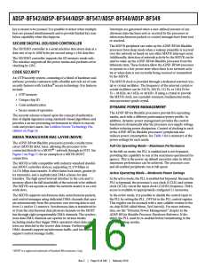
Power Domains
2.7V TO 3.6V
INPUT VOLTAGE
RANGE
SET OF DECOUPLING
CAPACITORS
V
DDVR
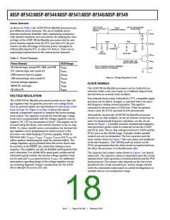
As shown in Table 6, the ADSP-BF54x Blackfin processors sup-
port different power domains. The use of multiple power
domains maximizes flexibility while maintaining compliance
with industry standards and conventions. By isolating the inter-
nal logic of the ADSP-BF54x Blackfin processors into its own
power domain separate from the RTC and other I/O, the pro-
cessors can take advantage of dynamic power management
without affecting the RTC or other I/O devices. There are no
sequencing requirements for the various power domains.
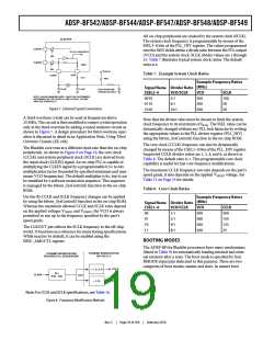
(LOW-INDUCTANCE)
V
V
DDVR
10μH
100nF
DDINT
+
+
100μF
FDS9431A
100μF
10μF
LOW ESR
ZHCS1000
VR
VR
OUT
OUT
Table 6. Power Domains
SHORT AND LOW-
INDUCTANCE WIRE
Power Domain
VDD Range
VDDINT
NOTE: DESIGNER SHOULD MINIMIZE
TRACE LENGTH TO FDS9431A.
All internal logic, except RTC, DDR, and USB
RTC internal logic and crystal I/O
DDR external memory supply
USB internal logic and crystal I/O
Internal voltage regulator
MXVR PLL and logic
GND
VDDRTC
VDDDDR
VDDUSB
VDDVR
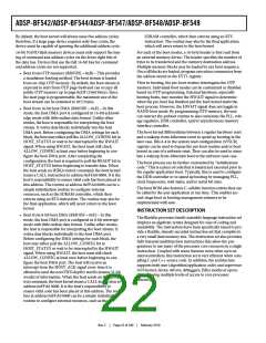
Figure 6. Voltage Regulator Circuit
CLOCK SIGNALS
VDDMP
The ADSP-BF54x Blackfin processors can be clocked by an
external crystal, a sine wave input, or a buffered, shaped clock
derived from an external clock oscillator.
If an external clock is used, it should be a TTL-compatible signal
and must not be halted, changed, or operated below the speci-
fied frequency during normal operation. This signal is
connected to the processor’s CLKIN pin. When an external
clock is used, the XTAL pin must be left unconnected.
Alternatively, because the ADSP-BF54x Blackfin processors
include an on-chip oscillator circuit, an external crystal may be
used. For fundamental frequency operation, use the circuit
shown in Figure 7. A parallel-resonant, fundamental frequency,
microprocessor-grade crystal is connected across the CLKIN
and XTAL pins. The on-chip resistance between CLKIN and the
XTAL pin is in the 500 kΩ range. Typically, further parallel
resistors are not recommended. The two capacitors and the
series resistor shown in Figure 7 fine-tune phase and amplitude
of the sine frequency. The 1MOhm pull-up resistor on the
XTAL pin guarantees that the clock circuit is properly held inac-
tive when the processor is in the hibernate state.
The capacitor and resistor values shown in Figure 7 are typical
values only. The capacitor values are dependent upon the crystal
manufacturers’ load capacitance recommendations and the PCB
physical layout. The resistor value depends on the drive level
specified by the crystal manufacturer. System designs should
verify the customized values based on careful investigations on
multiple devices over temperature range.
All other I/O
VDDEXT
VOLTAGE REGULATION
The ADSP-BF54x Blackfin processors provide an on-chip volt-
age regulator that can generate processor core voltage levels
from an external supply (see specifications in Operating Condi-
tions on Page 34). Figure 6 on Page 18 shows the typical
external components required to complete the power manage-
ment system. The regulator controls the internal logic voltage
levels and is programmable with the voltage regulator control
register (VR_CTL) in increments of 50 mV. This register can be
accessed using the bfrom_SysControl() function in the on-chip
ROM. To reduce standby power consumption, the internal volt-
age regulator can be programmed to remove power to the
processor core while keeping I/O power supplied. While in
hibernate state, VDDEXT, VDDRTC, VDDDDR, VDDUSB, and VDDVR can
still be applied, eliminating the need for external buffers. The
voltage regulator can be activated from this power-down state
by assertion of the RESET pin, which then initiates a boot
sequence. The regulator can also be disabled and bypassed at the
user’s discretion. For all 600 MHz speed grade models and all
automotive grade models, the internal voltage regulator must
not be used and VDDVR must be tied to VDDEXT. For additional
information regarding design of the voltage regulator circuit,
see Switching Regulator Design Considerations for the ADSP-
BF533 Blackfin Processors (EE-228).
Rev. C
|
Page 18 of 100
|
February 2010

 ADI [ ADI ]