ADSP-BF542/ADSP-BF544/ADSP-BF547/ADSP-BF548/ADSP-BF549
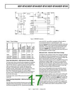
5.0V
1.25V
600Z
MOST FOT
RXVCC
RXGND
VDDINT
ADSP-BF549
10k6
GND
PG11/MTXON
MOST
600Z
NETWORK
600Z
TXVCC
TXGND
XN4114
VDDMP
MF
0.01
0.1MF
276
TX_DATA
RX_DATA
STATUS
PH5/MTX
PH6/MRX
GNDMP
0 6
MXO
MXI
PH7/MRXON
24.576MHz
PC4/RFS0
MFS
6
33
L/RCLK
MCLK
AUDIO DAC
336
336
PC1/MMCLK
PC5/MBCLK
MLF_P
MLF_M
BCLK
AUDIO
R1
CHANNELS
C2
330 6 1%
PC3/TSCLK0
PC7/RSCLK0
330pF
2% PPS
C1
MF
0.047
SDATA
PC2/DT0PRI
2% PPS
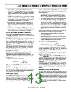
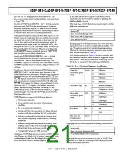
Figure 5. MXVR MOST Connection
Table 5. Power Settings
such as the RTC, may still be running but will not be able to
access internal resources or external memory. This
powered-down mode can only be exited by assertion of the reset
interrupt (RESET) or by an asynchronous interrupt generated
by the RTC. In deep sleep mode, an asynchronous RTC inter-
rupt causes the processor to transition to the active mode.
Assertion of RESET while in deep sleep mode causes the proces-
sor to transition to the full on mode.
Full On
Active
Enabled
No
Enabled Enabled On
Enabled Enabled On
Enabled/ Yes
Disabled
Hibernate State—Maximum Static Power Savings
Sleep
Enabled
-
-
-
Disabled Enabled On
Disabled Disabled On
Disabled Disabled Off
The hibernate state maximizes static power savings by disabling
the voltage and clocks to the processor core (CCLK) and to all
the synchronous peripherals (SCLK). The internal voltage regu-
lator for the processor can be shut off by using the
Deep Sleep Disabled
Hibernate Disabled
bfrom_SysControl() function in the on-chip ROM. This sets the
internal power supply voltage (VDDINT) to 0 V to provide the
greatest power savings mode. Any critical information stored
internally (memory contents, register contents, and so on) must
be written to a non-volatile storage device prior to removing
power if the processor state is to be preserved.
Since VDDEXT is still supplied in this mode, all of the external
pins three-state, unless otherwise specified. This allows other
devices that may be connected to the processor to have power
still applied without drawing unwanted current.
The internal supply regulator can be woken up by CAN, by the
MXVR, by the keypad, by the up/down counter, by the USB,
and by some GPIO pins. It can also be woken up by a real-time
clock wakeup event or by asserting the RESET pin. Waking up
from hibernate state initiates the hardware reset sequence.
With the exception of the VR_CTL and the RTC registers, all
internal registers and memories lose their content in hibernate
state. State variables may be held in external SRAM or DDR
memory.
Sleep Operating Mode—High Dynamic Power Savings
The sleep mode reduces dynamic power dissipation by disabling
the clock to the processor core (CCLK). The PLL and system
clock (SCLK), however, continue to operate in this mode. Typi-
cally an external event or RTC activity will wake up the
processor. In the sleep mode, assertion of a wakeup event
enabled in the SIC_IWRx register causes the processor to sense
the value of the BYPASS bit in the PLL control register
(PLL_CTL). If BYPASS is disabled, the processor transitions to
the full on mode. If BYPASS is enabled, the processor transi-
tions to the active mode.
In the sleep mode, system DMA access to L1 memory is not
supported.
Deep Sleep Operating Mode—Maximum Dynamic Power
Savings
The deep sleep mode maximizes dynamic power savings by dis-
abling the clocks to the processor core (CCLK) and to all
synchronous peripherals (SCLK). Asynchronous peripherals,
Rev. C
|
Page 17 of 100
|
February 2010

 ADI [ ADI ]