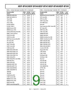
ADSP-BF542/ADSP-BF544/ADSP-BF547/ADSP-BF548/ADSP-BF549
• Companding in hardware. Each SPORT can perform
includes support for five to eight data bits, one or two stop bits,
and none, even, or odd parity. Each UART port supports two
modes of operation:
• PIO (programmed I/O). The processor sends or receives
data by writing or reading I/O-mapped UART registers.
The data is double-buffered on both transmit and receive.
• DMA (direct memory access). The DMA controller trans-
fers both transmit and receive data. This reduces the
number and frequency of interrupts required to transfer
data to and from memory. Each UART has two dedicated
DMA channels, one for transmit and one for receive. These
DMA channels have lower default priority than most DMA
channels because of their relatively low service rates. Flexi-
ble interrupt timing options are available on the transmit
side.
Each UART port’s baud rate, serial data format, error code gen-
eration and status, and interrupts are programmable:
• Supporting bit rates ranging from (fSCLK/1,048,576) to
(fSCLK) bits per second.
• Supporting data formats from seven to 12 bits per frame.
• Both transmit and receive operations can be configured to
generate maskable interrupts to the processor.
A-law or μ-law companding according to ITU recommen-
dation G.711. Companding can be selected on the transmit
and/or receive channel of the SPORT without additional
latencies.
• DMA operations with single-cycle overhead. Each SPORT
can receive and transmit multiple buffers of memory data
automatically. The processor can link or chain sequences of
DMA transfers between a SPORT and memory.
• Interrupts. Each transmit and receive port generates an
interrupt upon completing the transfer of a data word or
after transferring an entire data buffer or buffers through
DMA.
• Multichannel capability. Each SPORT supports 128 chan-
nels out of a 1024-channel window and is compatible with
the H.100, H.110, MVIP-90, and HMVIP standards.
SERIAL PERIPHERAL INTERFACE (SPI) PORTS
The ADSP-BF54x Blackfin processors have up to three SPI-
compatible ports that allow the processor to communicate with
multiple SPI-compatible devices.
Each SPI port uses three pins for transferring data: two data pins
(master output slave input, SPIxMOSI, and master input-slave
output, SPIxMISO) and a clock pin (serial clock, SPIxSCK). An
SPI chip select input pin (SPIxSS) lets other SPI devices select
the processor, and three SPI chip select output pins per SPI port
SPIxSELy let the processor select other SPI devices. The SPI
select pins are reconfigured general-purpose I/O pins. Using
these pins, the SPI ports provide a full-duplex, synchronous
serial interface, which supports both master/slave modes and
multimaster environments.
The SPI port’s baud rate and clock phase/polarities are pro-
grammable, and it has an integrated DMA controller,
configurable to support transmit or receive data streams. The
SPI’s DMA controller can only service unidirectional accesses at
any given time.
The UART port’s clock rate is calculated as
f
SCLK
-----------------------------------------------------------------------------
UART Clock Rate =
(1 – EDBO)
16
× UART_Divisor
Where the 16-bit UART divisor comes from the UARTx_DLH
register (most significant 8 bits) and UARTx_DLL register (least
significant eight bits), and the EDBO is a bit in the
UARTx_GCTL register.
In conjunction with the general-purpose timer functions, auto-
baud detection is supported.
UART1 and UART3 feature a pair of UARTxRTS (request to
send) and UARTxCTS (clear to send) signals for hardware flow
purposes. The transmitter hardware is automatically prevented
from sending further data when the UARTxCTS input is de-
asserted. The receiver can automatically de-assert its
UARTxRTS output when the enhanced receive FIFO exceeds a
certain high-water level. The capabilities of the UARTs are fur-
ther extended with support for the Infrared Data Association
(IrDA®) Serial Infrared Physical Layer Link Specification (SIR)
protocol.
The SPI port’s clock rate is calculated as
f
SCLK
-----------------------------------
SPI Clock Rate =
2 × SPI_BAUD
Where the 16-bit SPI_BAUD register contains a value of
2 to 65,535.
During transfers, the SPI port transmits and receives simulta-
neously by serially shifting data in and out on its two serial data
lines. The serial clock line synchronizes the shifting and sam-
pling of data on the two serial data lines.
CONTROLLER AREA NETWORK (CAN)
The ADSP-BF54x Blackfin processors offer up to two CAN con-
trollers that are communication controllers that implement the
controller area network (CAN) 2.0B (active) protocol. This pro-
tocol is an asynchronous communications protocol used in both
industrial and automotive control systems. The CAN protocol is
well suited for control applications due to its capability to com-
municate reliably over a network since the protocol
UART PORTS (UARTS)
The ADSP-BF54x Blackfin processors provide up to four full-
duplex universal asynchronous receiver/transmitter (UART)
ports. Each UART port provides a simplified UART interface to
other peripherals or hosts, supporting full-duplex, DMA-sup-
ported, asynchronous transfers of serial data. A UART port
incorporates CRC checking, message error tracking, and fault
node confinement.
Rev. C
|
Page 13 of 100
|
February 2010

 ADI [ ADI ]