AD9268
When the device is in SPI mode, the PDWN and OEB pins
remain active. For SPI control of output enable and power-down,
the OEB and PDWN pins should be set to their default states.
HARDWARE INTERFACE
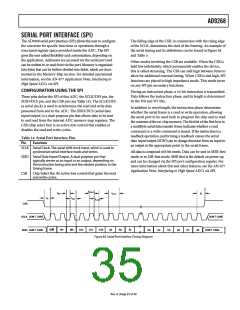
The pins described in Table 14 comprise the physical interface
between the user programming device and the serial port of the
AD9268. The SCLK pin and the CSB pin function as inputs
when using the SPI. The SDIO pin is bidirectional, functioning
as an input during write phases and as an output during
readback.
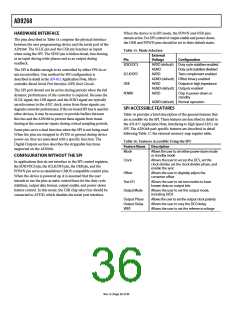
Table 15. Mode Selection
External
Voltage
Pin
Configuration
SDIO/DCS
AVDD (default) Duty cycle stabilizer enabled
AGND
AVDD
Duty cycle stabilizer disabled
Twos complement enabled
The SPI is flexible enough to be controlled by either FPGAs or
microcontrollers. One method for SPI configuration is
described in detail in the AN-812 Application Note, Micro-
controller-Based Serial Port Interface (SPI) Boot Circuit.
SCLK/DFS
OEB
AGND (default) Offset binary enabled
AVDD Outputs in high impedance
AGND (default) Outputs enabled
AVDD
Chip in power-down or
standby
AGND (default) Normal operation
The SPI port should not be active during periods when the full
dynamic performance of the converter is required. Because the
SCLK signal, the CSB signal, and the SDIO signal are typically
asynchronous to the ADC clock, noise from these signals can
degrade converter performance. If the on-board SPI bus is used for
other devices, it may be necessary to provide buffers between
this bus and the AD9268 to prevent these signals from transi-
tioning at the converter inputs during critical sampling periods.
PDWN
SPI ACCESSIBLE FEATURES
Table 16 provides a brief description of the general features that
are accessible via the SPI. These features are described in detail in
the AN-877 Application Note, Interfacing to High Speed ADCs via
SPI. The AD9268 part-specific features are described in detail
following Table 17, the external memory map register table.
Some pins serve a dual function when the SPI is not being used.
When the pins are strapped to AVDD or ground during device
power-on, they are associated with a specific function. The
Digital Outputs section describes the strappable functions
supported on the AD9268.
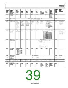
Table 16. Features Accessible Using the SPI
Feature Name
Description
Mode
Allows the user to set either power-down mode
or standby mode
Allows the user to access the DCS, set the
clock divider, set the clock divider phase, and
enable the sync
Allows the user to digitally adjust the
converter offset
Allows the user to set test modes to have
known data on output bits
Allows the user to set the output mode,
including LVDS
Allows the user to set the output clock polarity
Allows the user to vary the DCO delay
CONFIGURATION WITHOUT THE SPI
Clock
In applications that do not interface to the SPI control registers,
the SDIO/DCS pin, the SCLK/DFS pin, the OEB pin, and the
PDWN pin serve as standalone CMOS-compatible control pins.
When the device is powered up, it is assumed that the user
intends to use the pins as static control lines for the duty cycle
stabilizer, output data format, output enable, and power-down
feature control. In this mode, the CSB chip select bar should be
connected to AVDD, which disables the serial port interface.
Offset
Test I/O
Output Mode
Output Phase
Output Delay
VREF
Allows the user to set the reference voltage
Rev. A | Page 36 of 44

 ADI [ ADI ]