AD9268
ignore the rest. The clock divider sync enable bit (Address 0x100,
Bit 1) resets after it syncs.
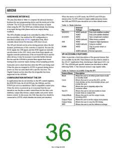
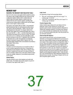
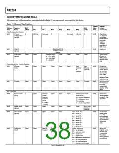
MEMORY MAP REGISTER DESCRIPTIONS
For additional information about functions controlled in
Register 0x00 to Register 0xFF, see the AN-877 Application Note,
Interfacing to High Speed ADCs via SPI.
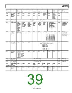
Bit 1—Clock Divider Sync Enable
Bit 1 gates the sync pulse to the clock divider. The sync signal is
enabled when Bit 1 is high and Bit 0 is high. This is continuous
sync mode.
Sync Control (Register 0x100)
Bits[7:3]—Reserved
Bit 0—Master Sync Enable
Bit 2—Clock Divider Next Sync Only
Bit 0 must be high to enable any of the sync functions. If the
sync capability is not used this bit should remain low to
conserve power.
If the master sync enable bit (Address 0x100, Bit 0) and the clock
divider sync enable bit (Address 0x100, Bit 1) are high, Bit 2 allows
the clock divider to sync to the first sync pulse it receives and to
Rev. A | Page 4± of 44

 ADI [ ADI ]