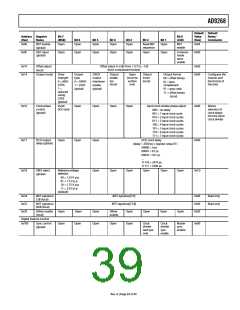
AD9268
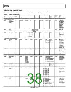
Default Default
Address Register
Bit 7
(MSB)
Bit 0
(LSB)
Value
(Hex)
Notes/
Comments
(Hex)
Name
Bit 6
Bit 5
Bit 4
Bit 3
Bit 2
Bit 1
±x±E
BIST enable
(global)
Open
Open
Open
Open
Open
Open
Reset BIST
sequence
Open
BIST
enable
±x±4
±x±F
ADC input
(global)
Open
Open
Open
Open
Open
Open
Common-
mode
±x±±
servo
enable
±x1±
±x14
Offset adjust
(local)
Offset adjust in LSBs from +12ꢁ to −128
(twos complement format)
±x±±
±x±±
Output mode
Drive
Output
type
± = CMOS
1 = LVDS
(global)
CMOS
Output
enable
bar
Open
(must be
written
low)
Output
invert
(local)
Output format
±± = offset binary
±1 = twos
complement
±1 = gray code
11 = offset binary
(local)
Configures the
outputs and
the format of
the data
strength
± = ANSI
LVDS;
output
interleave
enable
(global)
(local)
1 =
reduced
swing
LVDS
(global)
±x16
Clock phase
control
(global)
Invert
DCO clock
Open
Open
Open
Open
Input clock divider phase adjust
±±± = no delay
±x±±
Allows
selection of
clock delays
into the input
clock divider
±±1 = 1 input clock cycle
±1± = 2 input clock cycles
±11 = 3 input clock cycles
1±± = 4 input clock cycles
1±1 = ꢀ input clock cycles
11± = 6 input clock cycles
111 = ꢁ input clock cycles
±x1ꢁ
DCO output
Open
Open
Open
DCO clock delay
±x±±
delay (global)
(delay = 2ꢀ±± ps × register value/31)
±±±±± = ± ps
±±±±1 = 81 ps
±±±1± = 161 ps
…
1111± = 2419 ps
11111 = 2ꢀ±± ps
±x18
VREF select
(global)
Reference voltage
selection
Open
Open
Open
Open
Open
Open
±xC±
±± = 1.2ꢀ V p-p
±1 = 1.ꢀ V p-p
1± = 1.ꢁꢀ V p-p
11 = 2.± V p-p
(default)
±x24
±x2ꢀ
±x3±
BIST signature
LSB (local)
BIST signature[ꢁ:±]
BIST signature[1ꢀ:8]
±x±±
±x±±
±x±±
Read only
Read only
BIST signature
MSB (local)
Dither enable
(local)
Open
Open
Open
Open
Open
Dither
Open
Open
Open
Open
enable
Digital Feature Control
±x1±±
Sync control
(global)
Open
Open
Open
Clock
Clock
divider
sync
Master
sync
enable
±x±±
divider
next sync
only
enable
Rev. A | Page 39 of 44

 ADI [ ADI ]