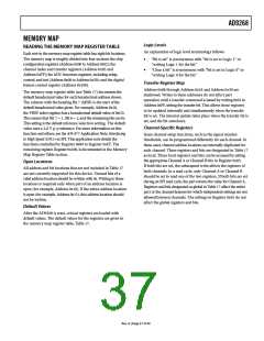
AD9268
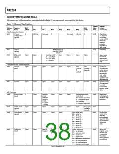
MEMORY MAP REGISTER TABLE
All address and bit locations that are not included in Table 17 are not currently supported for this device.
Table 17. Memory Map Registers
Default Default
Address Register
(Hex) Name
Chip Configuration Registers
Bit 7
(MSB)
Bit 0
(LSB)
Value
(Hex)
Notes/
Comments
Bit 6
Bit 5
Bit 4
Bit 3
Bit 2
Bit 1
±x±±
SPI port
configuration
(global)
±
LSB first
Soft reset
1
1
Soft reset
LSB first
±
±x18
The nibbles
are mirrored
so LSB-first
mode or MSB-
first mode
registers
correctly,
regardless of
shift mode
±x±1
±x±2
Chip ID
(global)
8-bit Chip ID[ꢁ:±]
(AD9268 = ±x32)
(default)
±x32
Read only
Chip grade
(global)
Open
Open
Open
Speed grade ID
±1 = 12ꢀ MSPS
Open
Open
Open
Open
Open
Speed grade
ID used to
differentiate
devices; read
only
1± = 1±ꢀ MSPS
11 = 8± MSPS
Channel Index and Transfer Registers
±x±ꢀ
Channel
index
Open
Open
Open
Open
Data
Channel
B
Data
Channel A
(default)
±x±3
Bits are set
to determine
which device
on the chip
receives the
next write
(default)
command;
applies to local
registers only
±xFF
Transfer
Open
Open
Open
Open
Open
Open
Open
Open
Open
Open
Open
Transfer
±x±±
±x8±
Synchronously
transfers data
from the
master shift
register to the
slave
ADC Functions
±x±8
Power modes
(local)
1
External
power-
down pin
function
(local)
± = pdwn
1 = stndby
Open
Internal power-down
mode (local)
±± = normal operation
±1 = full power-down
1± = standby
Determines
various generic
modes of chip
operation
11 = normal operation
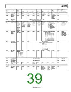
±x±9
±x±B
Global clock
(global)
Open
Open
Open
Open
Open
Open
Open
Open
Open
Open
Duty cycle
stabilizer
(default)
±x±1
±x±±
Clock divide
(global)
Open
Clock divide ratio
±±± = divide by 1
±±1 = divide by 2
±1± = divide by 3
±11 = divide by 4
1±± = divide by ꢀ
1±1 = divide by 6
11± = divide by ꢁ
111 = divide by 8
Clock divide
values other
than ±±±
automatically
cause the duty
cycle stabilizer
to become
active
±x±D
Test mode
(local)
Open
Open
Reset PN
long gen
Reset
PN short
gen
Open
Output test mode
±±± = off (default)
±±1 = midscale short
±1± = positive FS
±11 = negative FS
1±± = alternating checkerboard
1±1 = PN long sequence
11± = PN short sequence
111 = one/zero word toggle
±x±±
When this
register is set,
the test data
is placed on
the output
pins in place of
normal data
Rev. A | Page 38 of 44

 ADI [ ADI ]