AD9268
MEMORY MAP
READING THE MEMORY MAP REGISTER TABLE
Logic Levels
An explanation of logic level terminology follows:
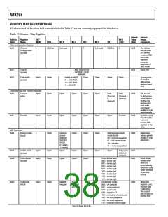
Each row in the memory map register table has eight bit locations.
The memory map is roughly divided into four sections: the chip
configuration registers (Address 0x00 to Address 0x02); the
channel index and transfer registers (Address 0x05 and
Address 0xFF); the ADC functions registers, including setup,
control, and test (Address 0x08 to Address 0x30); and the digital
feature control register (Address 0x100).
•
“Bit is set” is synonymous with “bit is set to Logic 1” or
“writing Logic 1 for the bit.”
•
“Clear a bit” is synonymous with “bit is set to Logic 0” or
“writing Logic 0 for the bit.”
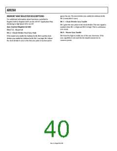
Transfer Register Map
Address 0x08 through Address 0x18 and Address 0x30 are
shadowed. Writes to these addresses do not affect part
operation until a transfer command is issued by writing 0x01 to
Address 0xFF, setting the transfer bit. This allows these registers
to be updated internally and simultaneously when the transfer
bit is set. The internal update takes place when the transfer bit is
set, and the bit autoclears.
The memory map register table (see Table 17) documents the
default hexadecimal value for each hexadecimal address shown.
The column with the heading Bit 7 (MSB) is the start of the
default hexadecimal value given. For example, Address 0x18,
the VREF select register, has a hexadecimal default value of 0xC0.
This means that Bit 7 = 1, Bit 6 = 1, and the remaining bits are 0s.
This setting is the default reference selection setting. The default
value uses a 2.0 V p-p reference. For more information on this
function and others, see the AN-877 Application Note, Interfacing
to High Speed ADCs via SPI. This application note details the
functions controlled by Register 0x00 to Register 0xFF. The
remaining register, Register 0x100, is documented in the Memory
Map Register Table section.
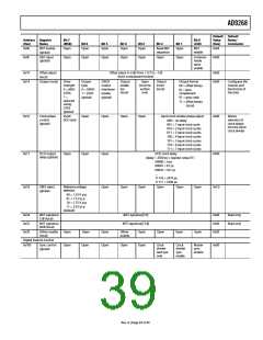
Channel-Specific Registers
Some channel setup functions, such as the signal monitor
thresholds, can be programmed differently for each channel. In
these cases, channel address locations are internally duplicated for
each channel. These registers and bits are designated in Table 17
as local. These local registers and bits can be accessed by setting
the appropriate Channel A or Channel B bits in Register 0x05.
If both bits are set, the subsequent write affects the registers of
both channels. In a read cycle, only Channel A or Channel B
should be set to read one of the two registers. If both bits are set
during an SPI read cycle, the part returns the value for Channel A.
Registers and bits designated as global in Table 17 affect the entire
part or the channel features for which independent settings are not
allowed between channels. The settings in Register 0x05 do not
affect the global registers and bits.
Open Locations
All address and bit locations that are not included in Table 17
are not currently supported for this device. Unused bits of a
valid address location should be written with 0s. Writing to these
locations is required only when part of an address location is
open (for example, Address 0x18). If the entire address location
is open (for example, Address 0x13), this address location should
not be written.
Default Values
After the AD9268 is reset, critical registers are loaded with
default values. The default values for the registers are given in
the memory map register table, Table 17.
Rev. A | Page 3ꢁ of 44

 ADI [ ADI ]