AD9228
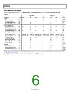
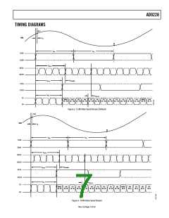
SWITCHING SPECIFICATIONS
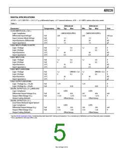
AVDD = 1.8 V, DRVDD = 1.8 V, 2 V p-p differential input, 1.0 V internal reference, AIN = −0.5 dBFS, unless otherwise noted.
Table 4.
AD9228-40
Typ
AD9228-65
Typ
Parameter1
CLOCK2
Temp
Min
Max
Min
Max
Unit
Maximum Clock Rate
Minimum Clock Rate
Full
Full
Full
Full
ꢁ0
ꢃ5
MSPS
MSPS
ns
10
10
Clock Pulse Width High (tEH
)
12.5
12.5
ꢂ.ꢂ
ꢂ.ꢂ
Clock Pulse Width Low (tEL)
ns
OUTPUT PARAMETERS2
Propagation Delay (tPD
)
Full
Full
Full
Full
Full
2.0
2.0
2.ꢂ
3.5
3.5
2.0
2.0
2.ꢂ
3.5
3.5
ns
ps
ps
ns
ns
Rise Time (tR) (20% to ꢀ0%)
Fall Time (tF) (20% to ꢀ0%)
FCO Propagation Delay (tFCO
300
300
2.ꢂ
300
300
2.ꢂ
)
3
DCO Propagation Delay (tCPD
)
tFCO
+
tFCO
+
(tSAMPLE/2ꢁ)
(tSAMPLE/2ꢁ)
3
Full
Full
Full
(tSAMPLE/2ꢁ) − 300 (tSAMPLE/2ꢁ) (tSAMPLE/2ꢁ) + 300 (tSAMPLE/2ꢁ) − 300 (tSAMPLE/2ꢁ) (tSAMPLE/2ꢁ) + 300 ps
(tSAMPLE/2ꢁ) − 300 (tSAMPLE/2ꢁ) (tSAMPLE/2ꢁ) + 300 (tSAMPLE/2ꢁ) − 300 (tSAMPLE/2ꢁ) (tSAMPLE/2ꢁ) + 300 ps
DCO to Data Delay (tDATA
)
3
DCO to FCO Delay (tFRAME
Data to Data Skew
)
50
150
50
150
ps
(tDATA-MAX − tDATA-MIN
)
Wake-Up Time (Standby)
25°C
25°C
Full
ꢃ00
3ꢂ5
10
ꢃ00
3ꢂ5
10
ns
μs
Wake-Up Time (Power Down)
Pipeline Latency
CLK
cycles
APERTURE
Aperture Delay (tA)
25°C
25°C
25°C
500
<1
1
500
<1
2
ps
Aperture Uncertainty (Jitter)
Out-of-Range Recovery Time
ps rms
CLK
cycles
1 See the AN-ꢀ35 Application Note, “Understanding High Speed ADC Testing and Evaluation,” for a complete set of definitions and how these tests were completed.
2 Can be adjusted via the SPI interface.
3 tSAMPLE/2ꢁ is based on the number of bits divided by 2 because the delays are based on half duty cycles.
Rev. 0 | Page ꢃ of 52

 ADI [ ADI ]