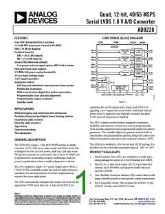
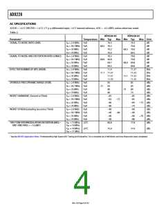
AD9228
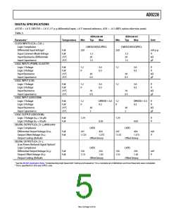
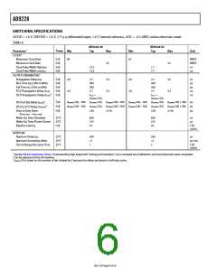
DIGITAL SPECIFICATIONS
AVDD = 1.8 V, DRVDD = 1.8 V, 2 V p-p differential input, 1.0 V internal reference, AIN = −0.5 dBFS, unless otherwise noted.
Table 3.
AD9228-40
Typ Max
AD9228-65
Typ Max
Parameter1
Temperature
Min
Min
Unit
CLOCK INPUTS (CLK+, CLK−)
Logic Compliance
CMOS/LVDS/LVPECL
CMOS/LVDS/LVPECL
Differential Input Voltage2
Input Common-Mode Voltage
Input Resistance (Differential)
Input Capacitance
Full
Full
25°C
25°C
250
250
mV p-p
V
kΩ
pF
1.2
20
1.5
1.2
20
1.5
LOGIC INPUTS (PDWN, SCLK/DTP)
Logic 1 Voltage
Logic 0 Voltage
Input Resistance
Input Capacitance
Full
Full
25°C
25°C
1.2
0
3.ꢃ
0.3
1.2
1.2
3.ꢃ
0.3
V
V
kΩ
pF
30
0.5
30
0.5
LOGIC INPUT (CSB)
Logic 1 Voltage
Logic 0 Voltage
Full
Full
1.2
0
3.ꢃ
0.3
3.ꢃ
0.3
V
V
Input Resistance
Input Capacitance
25°C
25°C
ꢂ0
0.5
ꢂ0
0.5
kΩ
pF
LOGIC INPUT (SDIO/ODM)
Logic 1 Voltage
Logic 0 Voltage
Full
Full
1.2
0
DRVDD + 0.3 1.2
DRVDD + 0.3
0.3
V
V
0.3
0
Input Resistance
Input Capacitance
25°C
25°C
30
2
30
2
kΩ
pF
LOGIC OUTPUT (SDIO/ODM)
Logic 1 Voltage (IOH = 50 μA)
Logic 0 Voltage (IOL = 50 μA)
DIGITAL OUTPUTS (D+, D−), (ANSI-ꢃꢁꢁ)1
Logic Compliance
Full
Full
1.ꢂ9
1.ꢂ9
V
V
0.05
0.05
LVDS
LVDS
Differential Output Voltage (VOD
)
Full
Full
2ꢁꢂ
1.125
ꢁ5ꢁ
1.3ꢂ5
2ꢁꢂ
1.125
ꢁ5ꢁ
1.3ꢂ5
mV
V
Output Offset Voltage (VOS
)
Output Coding (Default)
Offset binary
Offset binary
DIGITAL OUTPUTS (D+, D−),
(Low Power, Reduced Signal Option)1
Logic Compliance
LVDS
LVDS
Differential Output Voltage (VOD
)
Full
Full
150
1.10
250
1.30
150
1.10
250
1.30
mV
V
Output Offset Voltage (VOS
)
Output Coding (Default)
Offset binary
Offset binary
1 See the AN-ꢀ35 Application Note, “Understanding High Speed ADC Testing and Evaluation,” for a complete set of definitions and how these tests were completed.
2 This is specified for LVDS and LVPECL only.
Rev. 0 | Page 5 of 52

 ADI [ ADI ]