AD9228
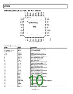
PIN CONFIGURATION AND FUNCTION DESCRIPTIONS
PIN 1
INDICATOR
AVDD
AVDD
VIN – D
VIN + D
AVDD
AVDD
CLK–
1
2
36
35
34
33
32
31
30
29
28
27
26
25
AVDD
AVDD
3
VIN – A
VIN + A
AVDD
EXPOSED PADDLE, PIN 0
(BOTTOM OF PACKAGE)
4
5
6
PDWN
AD9228
TOP VIEW
7
CSB
8
CLK+
SDIO/ODM
SCLK/DTP
AVDD
9
AVDD
AVDD
DRGND
DRVDD
10
11
12
DRGND
DRVDD
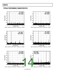
Figure 5. 48-Lead LFCSP Top View
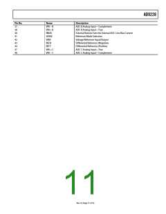
Table 7. Pin Function Descriptions
Pin No.
Name
Description
0
AGND
AVDD
Analog Ground (Exposed Paddle)
1.ꢀ V Analog Supply
1, 2, 5, ꢃ, 9, 10, 2ꢂ, 32,
35, 3ꢃ, 39, ꢁ5, ꢁꢃ
11, 2ꢃ
12, 25
3
ꢁ
ꢂ
DRGND
DRVDD
VIN − D
VIN + D
CLK−
Digital Output Driver Ground
1.ꢀ V Digital Output Driver Supply
ADC D Analog Input—Complement
ADC D Analog Input—True
Input Clock—Complement
Input Clock—True
ꢀ
CLK+
13
1ꢁ
15
1ꢃ
1ꢂ
1ꢀ
19
20
21
22
23
2ꢁ
2ꢀ
29
30
31
33
3ꢁ
D − D
D + D
D − C
D + C
D − B
D + B
D − A
D + A
ADC D Complement Digital Output
ADC D True Digital Output
ADC C Complement Digital Output
ADC C True Digital Output
ADC B Complement Digital Output
ADC B True Digital Output
ADC A Complement Digital Output
ADC A True Digital Output
Frame Clock Output—Complement
Frame Clock Output—True
Data Clock Output—Complement
Data Clock Output—True
Serial Clock/Digital Test Pattern
Serial Data Input-Output/Output Driver Mode
CSB
Power-Down
ADC A Analog Input—True
ADC A Analog Input—Complement
FCO−
FCO+
DCO−
DCO+
SCLK/DTP
SDIO/ODM
CSB
PDWN
VIN + A
VIN − A
Rev. 0 | Page 10 of 52

 ADI [ ADI ]