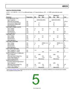
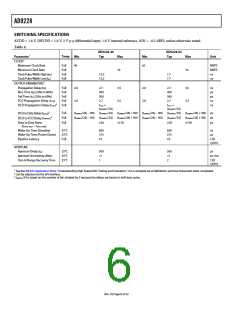
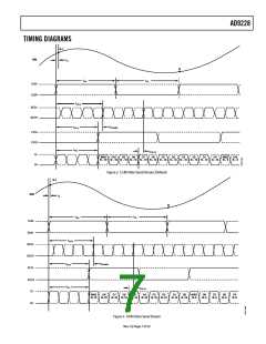
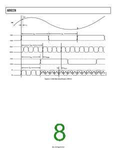
AD9228
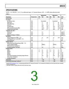
SPECIFICATIONS
AVDD = 1.8 V, DRVDD = 1.8 V, 2 V p-p differential input, 1.0 V internal reference, AIN = −0.5 dBFS, unless otherwise noted.
Table 1.
AD9228-40
Min Typ
AD9228-65
Max Min Typ
Parameter1
Temperature
Max
Unit
RESOLUTION
12
12
Bits
ACCURACY
No Missing Codes
Offset Error
Offset Matching
Gain Error
Full
Full
Full
Full
Full
Full
Full
Guaranteed
Guaranteed
1
2
2
0.3
0.3
0.ꢁ
1
2
0.ꢁ
0.3
0.25
0.ꢁ
ꢀ
ꢀ
1.2
0.ꢂ
0.5
1
ꢀ
mV
ꢀ
mV
3.5
0.ꢂ
% FS
% FS
Gain Matching
Differential Nonlinearity (DNL)
Integral Nonlinearity (INL)
TEMPERATURE DRIFT
Offset Error
Gain Error
Reference Voltage (1 V Mode)
REFERENCE
0.ꢃ5 LSB
1
LSB
Full
Full
Full
2
1ꢂ
21
2
1ꢂ
21
ppm/°C
ppm/°C
ppm/°C
Output Voltage Error (VREF = 1 V)
Load Regulation @ 1.0 mA (VREF = 1 V)
Input Resistance
Full
Full
Full
2
3
ꢃ
30
2
3
ꢃ
30
mV
mV
kΩ
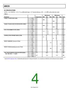
ANALOG INPUTS
Differential Input Voltage Range (VREF = 1 V)
Common-Mode Voltage
Differential Input Capacitance
Analog Bandwidth, Full Power
POWER SUPPLY
Full
Full
Full
Full
2
2
V p-p
V
pF
AVDD/2
ꢂ
315
AVDD/2
ꢂ
315
MHz
AVDD
DRVDD
IAVDD
IDRVDD
Full
Full
Full
Full
Full
Full
Full
Full
Full
1.ꢂ
1.ꢂ
1.ꢀ
1.ꢀ
155
31
335
2
1.9
1.ꢂ
1.ꢂ
1.ꢀ
1.ꢀ
232
3ꢁ
ꢁꢂꢀ
2
1.9
1.9
2ꢁ5
3ꢀ
510
5.ꢀ
V
V
1.9
1ꢂ0
3ꢁ
3ꢃꢂ
5.ꢀ
mA
mA
mW
mW
mW
dB
Total Power Dissipation (Including Output Drivers)
Power-Down Dissipation
Standby Dissipation2
CROSSTALK
ꢂ2
ꢂ2
−100
−100
−100
−100
CROSSTALK (Overrange Condition)3
dB
1 See the AN-ꢀ35 Application Note, “Understanding High Speed ADC Testing and Evaluation,” for a complete set of definitions and how these tests were completed.
2 Can be controlled via SPI.
3 Overrange condition is specific with ꢃ dB of the full-scale input range.
Rev. 0 | Page 3 of 52

 ADI [ ADI ]