AD9228
TABLE OF CONTENTS
Features .............................................................................................. 1
Applications....................................................................................... 1
General Description......................................................................... 1
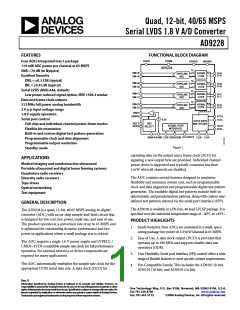
Functional Block Diagram .............................................................. 1
Product Highlights ........................................................................... 1
Revision History ............................................................................... 2
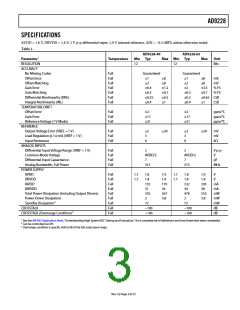
Specifications..................................................................................... 3
AC Specifications.......................................................................... 4
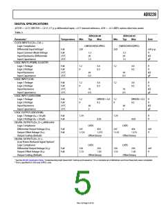
Digital Specifications ................................................................... 5
Switching Specifications .............................................................. 6
Timing Diagrams.............................................................................. 7
Absolute Maximum Ratings............................................................ 9
Thermal Impedance..................................................................... 9
ESD Caution.................................................................................. 9
Pin Configuration and Function Descriptions........................... 10
Equivalent Circuits......................................................................... 12
Typical Performance Characteristics ........................................... 14
Theory of Operation ...................................................................... 19
Analog Input Considerations ................................................... 19
Clock Input Considerations...................................................... 21
Serial Port Interface (SPI).............................................................. 29
Hardware Interface..................................................................... 29
Memory Map .................................................................................. 31
Reading the Memory Map Table.............................................. 31
Reserved Locations .................................................................... 31
Default Values............................................................................. 31
Logic Levels................................................................................. 31
Evaluation Board ............................................................................ 35
Power Supplies............................................................................ 35
Input Signals................................................................................ 35
Output Signals ............................................................................ 35
Default Operation and Jumper Selection Settings................. 36
Alternative Analog Input Drive Configuration...................... 37
Outline Dimensions....................................................................... 51
Ordering Guide .......................................................................... 51
REVISION HISTORY
4/06—Revision 0: Initial Version
Rev. 0 | Page 2 of 52

 ADI [ ADI ]