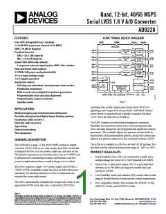
AD9228
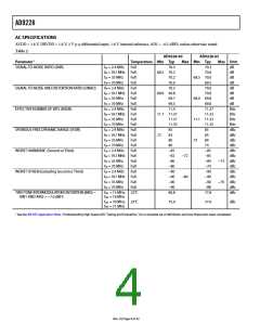
AC SPECIFICATIONS
AVDD = 1.8 V, DRVDD = 1.8 V, 2 V p-p differential input, 1.0 V internal reference, AIN = −0.5 dBFS, unless otherwise noted.
Table 2.
AD9228-40
AD9228-65
Parameter1
Temperature Min Typ Max Min Typ
Max Unit
dB
SIGNAL-TO-NOISE RATIO (SNR)
fIN = 2.ꢁ MHz
fIN = 19.ꢂ MHz Full
fIN = 35 MHz
fIN = ꢂ0 MHz
fIN = 2.ꢁ MHz
Full
ꢂ0.5
ꢃꢀ.5 ꢂ0.2
ꢂ0.2
ꢂ0.2
ꢂ0.0
ꢃꢀ.5 ꢂ0.0
ꢃ9.5
dB
dB
dB
Full
Full
Full
ꢂ0.0
SIGNAL-TO-NOISE AND DISTORTION RATIO (SINAD)
EFFECTIVE NUMBER OF BITS (ENOB)
ꢂ0.3
ꢃꢀ.0 ꢃ9.ꢀ
ꢃ9.ꢂ
ꢂ0.0
ꢂ0.0
ꢃꢀ.0 ꢃ9.ꢀ
ꢃ9.0
dB
dB
dB
dB
fIN = 19.ꢂ MHz Full
fIN = 35 MHz
fIN = ꢂ0 MHz
fIN = 2.ꢁ MHz
Full
Full
Full
ꢃ9.5
11.ꢁ
11.3ꢂ
Bits
fIN = 19.ꢂ MHz Full
11.1 11.3ꢂ
11.3ꢂ
11.33
11.1 11.33
11.25
Bits
Bits
Bits
fIN = 35 MHz
fIN = ꢂ0 MHz
fIN = 2.ꢁ MHz
Full
Full
Full
11.33
SPURIOUS-FREE DYNAMIC RANGE (SFDR)
WORST HARMONIC (Second or Third)
ꢀ5
ꢀ5
dBc
fIN = 19.ꢂ MHz Full
ꢂ2
ꢀ2
ꢀ0
ꢀ0
ꢀ5
ꢀꢁ
ꢂꢁ
dBc
dBc
dBc
fIN = 35 MHz
fIN = ꢂ0 MHz
fIN = 2.ꢁ MHz
Full
Full
Full
ꢂ3
−ꢀ5
−ꢀ2
−ꢀ0
−ꢀ0
−90
−90
−90
−90
ꢀ0.ꢀ
−ꢀ5
−ꢀ5
−ꢀꢁ
−ꢂꢁ
−90
−90
−90
−ꢀꢀ
ꢂꢂ.ꢀ
dBc
dBc
−ꢂ3 dBc
dBc
fIN = 19.ꢂ MHz Full
−ꢂ2
−ꢀ0
fIN = 35 MHz
fIN = ꢂ0 MHz
fIN = 2.ꢁ MHz
Full
Full
Full
WORST OTHER (Excluding Second or Third)
dBc
dBc
−ꢂ9 dBc
dBc
fIN = 19.ꢂ MHz Full
fIN = 35 MHz
fIN = ꢂ0 MHz
Full
Full
TWO-TONE INTERMODULATION DISTORTION (IMD)—
AIN1 AND AIN2 = −ꢂ.0 dBFS
fIN1 = 15 MHz, 25°C
IN2 = 1ꢃ MHz
fIN1 = ꢂ0 MHz, 25°C
IN2 = ꢂ1 MHz
dBc
f
ꢂ5.0
ꢂꢂ.0
dBc
f
1 See the AN-ꢀ35 Application Note, “Understanding High Speed ADC Testing and Evaluation,” for a complete set of definitions and how these tests were completed.
Rev. 0 | Page ꢁ of 52

 ADI [ ADI ]