AD7858/AD7858L
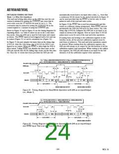
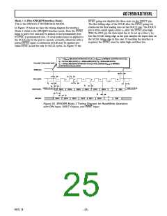
Mode 2 (3-Wire SPI/QSPI Interface Mode)
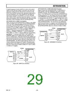
This is the DEFAULT INTERFACE MODE.
SYNC going low disables the three-state on the DOUT pin.
The first falling edge of the SCLK after the SYNC going low
clocks out the first leading zero on the DOUT pin. The DOUT
pin is three-stated again a time t12 after the SYNC goes high.
With the DIN pin the data input has to be set up a time t7 be-
fore the SCLK rising edge as the part samples the input data on
the SCLK rising edge in this case. If resetting the interface is
required, the SYNC must be taken high and then low.
In Figure 33 below we have the timing diagram for interface
Mode 2 which is the SPI/QSPI interface mode. Here the SYNC
input is active low and may be pulsed or tied permanently low.
If SYNC is permanently low, 16 clock pulses must be applied to
the SCLK pin for the part to operate correctly, otherwise with a
pulsed SYNC input a continuous SCLK may be applied pro-
vided SYNC is low for only 16 SCLK cycles. In Figure 33 the
t3 = –0.4tSCLK MIN (NONCONTINUOUS SCLK) ؎0.4tSCLK ns MIN/MAX (CONTINUOUS SCLK),
t6 = 75/115ns MAX (5V/3V), t7 = 40/60ns MIN (5V/3V), t8 = 20/30ns MIN (5V/3V),
t11 = 30/50ns MIN (NONCONTINUOUS SCLK) (5V/3V), (30/50)/0.4tSCLK ns MIN/MAX
(CONTINUOUS SCLK) (5V/3V)
POLARITY PIN LOGIC HIGH
SYNC (I/P)
t11
t3
t9
SCLK (I/P)
1
2
3
4
5
6
16
t10
t5
t12
t6
DB12
t6
THREE-STATE
THREE-STATE
DOUT (O/P)
DIN (I/P)
DB15
DB14
DB13
DB11
t8
DB10
DB10
DB0
t7
DB15
t8
DB14
DB13
DB12
DB11
DB0
Figure 33. SPI/QSPI Mode 2 Timing Diagram for Read/Write Operation
with DIN Input, DOUT Output, and SYNC Input
REV. B
–25–

 ADI [ ADI ]