AD7858/AD7858L
OPTIONAL
4MHz/1.8MHz
MICROPROCESSOR INTERFACING
AD7858/AD7858L
CONVST
In many applications, the user may not require the facility of
writing to most of the on-chip registers. The only writing neces-
sary is to set the input channel configuration. After this the
CONVST is applied, a conversion is performed, and the result
may be read using the SCLK to clock out the data from the
output register on to the DOUT pin. At the same time a write
operation occurs and this may consist of all 0s where no data is
written to the part or may set a different input channel configu-
ration for the next conversion. The SCLK may be connected to
the CLKIN pin if the user does not want to have to provide
separate serial and master clocks. With this arrangement the
SYNC signal must be low for 16 SCLK cycles for the read and
write operations.
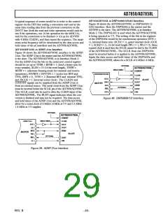
8XC51/L51
MASTER
CLKIN
P3.1
SCLK
SLAVE
P3.0
DIN
(INT0/P3.2)
BUSY
SYNC
OPTIONAL
Figure 37. 8XC51/PIC16C42 Interface
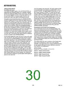
AD7858/AD7858L to 68HC11/16/L11/PIC16C42 Interface
Figure 38 shows the AD7858/AD7858L SPI/QSPI interface to
the 68HC11/16/L11/PIC16C42. The 68L11 is for interfacing to
the AD7858/AD7858L when the supply is 3 V. The AD7858/
AD7858L is in Interface Mode 2. The SYNC line is not used
and is tied to DGND. The µController is configured as the mas-
ter, by setting the MSTR bit in the SPCR to 1, and provides the
serial clock on the SCK pin. For all the µControllers the CPOL
bit is set to 1 and for the 68HC11/16/L11 the CPHA bit is set to
1. The CLKIN and CONVST signals can be supplied from the
µController or from separate sources. The BUSY signal can be
used as an interrupt to tell the µController when the conversion
is finished, then the reading and writing can take place. If re-
quired the reading and writing can take place during conversion
and there will be no need for the BUSY signal in this case.
CONVST
CONVERSION START
4MHz/1.8MHz
MASTER CLOCK
CLKIN
SCLK
SYNC SIGNAL TO
GATE THE SCLK
AD7858/
AD7858L
SYNC
SERIAL DATA INPUT
DIN
SERIAL DATA
OUTPUT
DOUT
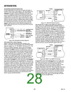
Figure 36. Simplified Interface Diagram
AD7858/AD7858L to 8XC51 Interface
Figure 37 shows the AD7858/AD7858L interface to the
8XC51. The 8XL51 is for interfacing to the AD7858/AD7858L
when the supply is at 3 V. The 8XC51 only runs at 5 V. The
8XC51 is in Mode 0 operation. This is a two-wire interface
consisting of the SCLK and the DIN which acts as a bidirec-
tional line. The SYNC is tied low. The BUSY line can be used
to give an interrupt driven system but this would not normally
be the case with the 8XC51. For the 8XC51 12 MHz version
the serial clock will run at a maximum of 1 MHz so the serial
interface of the AD7858/AD7858L will only be running at
1 MHz. The CLKIN signal must be provided separately to the
AD7858/AD7858L from a port line on the 8XC51 or from a
source other than the 8XC51. Here the SCLK cannot be tied to
the CLKIN as the SYNC is tied low permanently. The CONVST
signal can be provided from an external timer or conversion can
be started in software if required. The sequence of events would
typically be to write to the control register via the DIN line setting
a conversion start and the 2-wire interface mode (this would be
performed in two 8-bit writes), wait for the conversion to be
finished (4.6 µs with 4 MHz CLKIN), read the conversion result
data on the DIN line (this would be performed in two 8-bits
reads), and repeat the sequence. The maximum serial frequency
will be determined by the data access and hold times of the
8XC51 and the AD7858/AD7858L.
OPTIONAL
AD7858/AD7858L
CONVST
4MHz/1.8MHz
DV
DD
68HC11/L11/16
CLKIN
SYNC
SCLK
DOUT
SPI
SS
SLAVE
HC16, QSPI
OPTIONAL
SCK
MASTER
MISO
IRQ
BUSY
DIN
MOSI
Figure 38. 68HC11 and 68HC16 Interface
For the 68HC16 the word length should be set to 16 bits, and
the SS line should be tied to the SYNC pin for the QSPI inter-
face. The micro-sequencer and RAM associated with the
68HC16 QSPI port can be used to perform a number of read
and write operations, and store the conversion results in
memory, independent of the CPU. This is especially useful when
reading the conversion results from all eight channels consecu-
tively. The command section of the QSPI port RAM would be
programmed to perform a conversion on one channel, read the
conversion result, perform a conversion on the next channel,
read the conversion result, and so on until all eight conversion
results are stored into the QSPI RAM.
–28–
REV. B

 ADI [ ADI ]