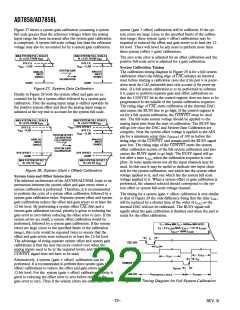
AD7858/AD7858L
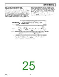
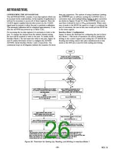
CONFIGURING THE AD7858/AD7858L
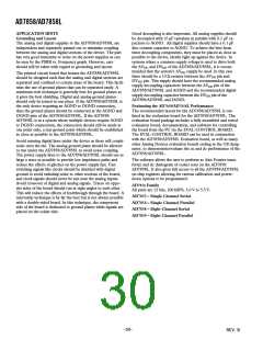
than one conversion. The options of using a hardware (pulsing
the CONVST pin) or software (setting the CONVST bit to 1)
conversion start, and reading/writing during or after conversion
are shown in Figures 34 and 35. If the CONVST pin is never
used then it should be tied to DVDD permanently. Where refer-
ence is made to the BUSY bit equal to a Logic 0, to indicate the
end of conversion, the user in this case would poll the BUSY bit
in the status register.
The AD7858/AD7858L contains 14 on-chip registers which can
be accessed via the serial interface. In the majority of applications it
will not be necessary to access all of these registers. Here the
CLKIN signal is applied directly after power-on; the CLKIN
signal must be present to allow the part to perform a calibration.
This automatic calibration will be completed approximately 32 ms
after the AD7858 has powered up (4 MHz CLK).
For accessing the on-chip registers it is necessary to write to the
part. To change the channel from the default channel setting
the user will be required to write to the part. To enable Serial
Interface Mode 1 the user must also write to the part. Figure 34
and 35 outline flowcharts of how to configure the AD7858/
AD7858L Serial Interface Modes 1 and 2 respectively. The
continuous loops on all diagrams indicate the sequence for more
Interface Mode 1 Configuration
Figure 34 shows the flowchart for configuring the part in Inter-
face Mode 1. This mode of operation can only be enabled by
writing to the control register and setting the 2/3 MODE bit.
Reading and writing cannot take place simultaneously in this
mode as the DIN pin is used for both reading and writing.
START
POWER-ON, APPLY CLKIN SIGNAL,
WAIT FOR AUTOMATIC CALIBRATION
SERIAL
INTERFACE
MODE
?
1
INITIATE
CONVERSION
YES
IN
SOFTWARE
?
NO
APPLY SYNC (IF REQUIRED), SCLK, WRITE
TO CONTROL REGISTER SETTING CHANNEL
TWO-WIRE MODE
APPLY SYNC (IF REQUIRED), SCLK,
WRITE TO CONTROL REGISTER
SETTING CHANNEL AND TWO-WIRE MODE
WRITE
TO CONTROL REGISTER SETTING CONVST
BIT TO 1 (SEE NOTE)
PULSE CONVST PIN
READ
DATA
DURING
CONVERSION
?
YES
WAIT APPROX. 200ns AFTER
CONVST RISING EDGE OR AFTER END
OF CONTROL REGISTER WRITE
NO
WAIT FOR BUSY SIGNAL TO GO LOW
OR
WAIT FOR BUSY BIT = 0
APPLY SYNC (IF REQUIRED), SCLK, READ
PREVIOUS CONVERSION RESULT ON DIN PIN
APPLY SYNC (IF REQUIRED), SCLK, READ
CURRENT CONVERSION RESULT ON DIN PIN
NOTE:
TWO SEPARATE WRITES ARE REQUIRED TO SET A NEW CHANNEL ADDRESS AND INITIATE A
CONVERSION ON THAT NEW CHANNEL IN SOFTWARE AS THE ACQUISITION TIME (2 tCLKIN
)
MUST ELAPSE BEFORE THE CONVERSION BEGINS. IF BOTH COMMANDS ARE ISSUED IN THE ONE
WRITE THE RESULT OF THIS CONVERSION SHOULD BE DISCARDED AND THE NEXT
CONVERSION ON THAT SAME CHANNEL WILL PROVIDE CORRECT RESULTS.
Figure 34. Flowchart for Setting Up, Reading, and Writing in Interface Mode 1
–26–
REV. B

 ADI [ ADI ]